ARM’s Mali Midgard Architecture Explored
by Ryan Smith on July 3, 2014 11:00 AM EST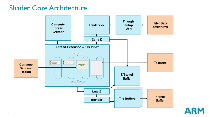
So far this is shaping up to be a banner year for SoCs. From a market perspective the mobile hardware space is still in a period of significant growth, but more importantly from a hardware point of view these products and especially the GPUs in these products have made significant strides in performance and in features. SoC GPUs will approach feature parity with desktop GPUs this year, and from a performance perspective they’re nearing the performance of the last-generation game consoles, a long-aspired goal given the “good enough” status attached to those devices.
Meanwhile at the same time that these products are maturing at a technical level, we’ve seen the various SoC firms mature at a professional level. The “wild west” days of SoCs have given way to mature markets of longer product cycles, longer product lives, and a more stable market overall. This both good and bad news for the various players in the SoC market as firms get squeezed out – SoC integrators such as TI and STMicroelectronics have been the first of such victims – but it also means that as companies become better established and more deeply entrenched, they can be more open about their projects and their products, and discuss them in greater detail than before without needing to be concerned about getting scooped by a competitor.
Here at AnandTech we’re particularly fond of doing architectural deep dives; our chance to talk to the people behind various processors and learn from them about how their products work and how they came together. Thanks to the maturation of the SoC market we’re finally getting a level of access in the SoC market that we haven’t had before, and in turn for the first time we get to tell the stories of the people behind these mind-bogglingly complex devices while better learning how they operate and as such how they compare. It’s admittedly a level of access we take for granted in the PC space, where companies such as Intel, AMD, and NVIDIA are regularly open, but it’s hard to contain our excitement about gaining this kind of access to the myriad of players in the SoC space.
This year then has been especially productive in that regard, and as of today it’s going to get even better. After we took a look at Imagination’s PowerVR Rogue architecture earlier this year, ARM contacted us and indicated that they would like to do the same; that they would like to take a seat at the “open architecture” table. To give us the access we need to discover how their GPUs work, and in turn tell you what we’ve learned.

To that end we’ve gladly let ARM pull up a seat, and today we’ll be taking our first in-depth look at ARM’s newest Mali SoC GPU architecture: Midgard. Now as with Imagination what we’re seeing today is most, but not all of the picture, as ARM has their secrets and they wish to keep some of them. But today we get to learn all about Midgard’s shader cores while also learning a thing or two about its pixel rendering pipeline, power optimizations, and other aspects of what makes Midgard tick. In other words, more than enough to keep us busy for one day.
But before we dive in we’d also like to quickly call attention to an Ask The Experts session we held with ARM’s Jem Davies, an ARM Fellow and VP of Technology in the Media Processing Division. While our deep dive is focusing on Midgard’s architecture, Jem has been answering all sorts of additional Mali-related questions, including business strategy and ARM’s views on GPU computing.
Finally, as this is the second article in our continuing series on SoC GPUs, we will be picking up from where we left off after our last article. While all of our articles are meant to be accessible to some degree, if you haven’t caught any of our previous articles I’d highly recommend our primer on how GPUs work for a quick overview of the technology before we dive into the nuts and bolts of ARM’s Midgard architecture.


66 Comments
View All Comments
LemmingOverlord - Thursday, July 3, 2014 - link
Quick suggestion: considering Adreno is one of the most widespread GPU architectures for mobile, could you edit the table in the last page to include Adreno 3xx/4xx GPUs?Thanks!
Anand Lal Shimpi - Tuesday, July 8, 2014 - link
Unfortunately Qualcomm refuses to disclose much detail about their GPU architectures. I completely disagree with their position and have worked on Qualcomm for years to get them to open up but at this point it's a meaningless effort.da_asmodai - Thursday, July 3, 2014 - link
How about adding the Qualcomms Adreno 420 to the comparison.Anand Lal Shimpi - Thursday, July 3, 2014 - link
I wish we could - Qualcomm refuses to disclose any deeper architectural details about any modern Adreno GPU architectures.Krysto - Thursday, July 3, 2014 - link
Their loss. Plus, neither Adreno 420 nor their upcoming CPU's look that interesting or competitive anyway. Adreno 420 should still give only about HALF the performance of Tegra K1's GPU.ChefJeff789 - Thursday, July 3, 2014 - link
Really? That's disappointing... I'm really looking forward to a time when ARM, nVidia, and AMD all compete on an architectural level in their GPUs, if it ever comes. The one-horse race with Intel in the desktop CPU space has been pretty lackluster for the past few years, in terms of performance increases. nVidia's Maxwell architecture seems pretty amazing in terms of efficiency, and I'm not yet convinced AMD will be able to compete. They have yet to impress with their APU and mobile processor efficiencies.frostyfiredude - Thursday, July 3, 2014 - link
Important to note that NVidia's TK1 will be achieving that double GFLOPS performance of the Adreno 420 at a clock speed of around 950Mhz. At that performance level the TDP is listed at <10W, so it's not exactly comparable to the S805 and Adreno 420 which target a TDP half as high. What I can see happening is the TK1 being able to stretch it's legs and thus being superior in large tablets but being too thermally crippled in phones and small tablets to reach those levels. Based on the previews I found, Adreno is more efficient in it's shader resource usage, closing that further.lmcd - Thursday, July 3, 2014 - link
That's actually pretty bad math there -- if the TK1 achieves double perf at double power, it should achieve the same perf at 1/4 power (well, not quite since it isn't as simple as the basic E&M I learned, but yeah).And by your logic still, why would the K1 not fit in phones and tablets even as the 420 manages?
tuxRoller - Friday, July 4, 2014 - link
Power is linear to f, but squares with V. I don't know that we can say that at half the f you can halve the V. Actually, that's almost certainly not the case, as it's not the case with any common processor tmk.tuxRoller - Thursday, July 3, 2014 - link
The adreno 420 provides around 220gflops. The 430 well then be over 300gflops. These are not counting changes in clock speed that could raise our lower performance.