3D and EDA need to make up for Moore’s Law, says Qualcomm
Qualcomm is looking to monolithic 3D (Guide) and smart circuit architectures to make up for the loss of traditional 2D process scaling as wafer costs for advanced nodes continue to increase. Speaking in a keynote at DAC 2014 in San Francisco, vice president of engineering Karim Arabi said improvements would be needed to allow the phone to overtake laptops in terms of performance.
“Mobile is becoming a centre of gravity for the user,” said Arabi. “It is providing a unique opportunity that no other device had in the past with. All these technologies provide opportunities but it becomes a challenge to develop because you have to integrate them at lower power and low cost as well.”
Arabi said he expected mobile SoCs to integrate more than ten billion transistors by 2020 but the technology to do that presents major issues. “One of the biggest problems is cost. We are very cost sensitive. Moore’s Law has been great. Now, although we are still scaling down it’s not cost-economic anymore. It’s creating a big problem for us,” he said.
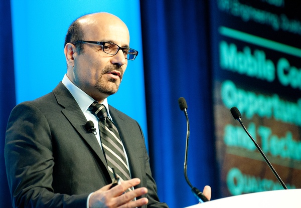
Image Qualcomm's Karim Arabi speaking at DAC 2014
Arabi pointed to interconnect as an important driver of a change in the approach to scaling: “Interconnect RC is inching up as we go to deeper technology. That is a major problem because designs are becoming interconnect-dominated. Something has to be done about interconnect. What needs to be done is monolithic three-dimensional ICs.”
This technology would be distinct from the current stacked chips, Arabi said: “Through-silicon vias and micro bumps are useful where you need I/Os. Those [board-level] I/Os are quite power hungry. If you want to replace those things, stacking is very good. And we see them in camera sensors or memory stacking. But they are not really solving the interconnect issue I’m talking about.
“So we are looking at true monolithic 3D. You have normal vias between different stacks. Then interconnect lengths will be smaller than with 2D. If we can connect between layers the delay becomes smaller. This is a technology for the end of the decade, but it can give us an advantage of one process node, with a 30 per cent power saving and a 40 per cent gain in performance,” Arabi claimed, turning to design.
“Moore’s law in my opinion is a self fulfilling prophecy. The industry is challenging itself to improve density by 2x. We are all working together to synchronise ourselves. It was easier to do with node scaling. While we did that, innovation with architecture and circuits slowed. Now that node scaling slowed down we have to turn on other aspects of scaling. Last but not least, it’s EDA. It’s time for EDA to really boost the innovation cycle to compensate for the slowdown.”
Arabi said he is looking to improved design techniques developed by the EDA industry to provide a 50 to 60 per cent reduction in area, as well as big improvements in design productivity. He cited design costs as a further major problem for organizations like Qualcomm. “We need a 10-20x gain in design productivity because it won’t be possible to increase the number of designers. We need a five to seven-fold reduction in power. And we need a 2x reduction in the overall design cycle. We need more disruptive innovation. We have some of the best talents working in EDA, so we can do it again.”
