


AppliedMicro Adopting TSMC 7nm FinFET Process Technology
AppliedMicro’s innovative silicon products enabled by TSMC’s advanced technology
SANTA CLARA, Calif., July 11, 2016 -- Applied Micro Circuits Corporation (NASDAQ:AMCC), a global leader in computing and connectivity solutions, today announced that it has adopted 7nm process technology from TSMC, the world’s leading foundry, to enable AppliedMicro’s innovative silicon products for cloud computing and networking applications.
“We are excited to extend our relationship with TSMC to ultimately bring cutting-edge technology to the cloud computing market,” said Paramesh Gopi, President and CEO of AppliedMicro. “We will work closely with TSMC to ensure our flagship silicon products benefit from their manufacturing excellence that is renowned throughout the industry. Together we will introduce technology to revolutionize the rapidly growing data-center market to deliver an unprecedented bundle of compute and connectivity performance, energy efficiency and bandwidth utilization at a low total cost of ownership.”
“We are pleased to be a part of AppliedMicro’s success,” said Dr. B.J. Woo, TSMC Vice President of Business Development. “TSMC’s advanced 7nm technology will empower AppliedMicro to deliver the critical performance needed in computing and connectivity applications.”
Recently introduced innovations from AppliedMicro include X-Gene® 3 at ARM TechCon in November 2015, and single lambda, mixed signal 100G X-Weave® PAM4 at the Optical Fiber Communications Conference in March 2016. Both product functions were validated with TSMC 16FF+ shuttle and are expected to sample to customers by early 2017.
About AppliedMicro
Applied Micro Circuits Corporation (NASDAQ:AMCC) is a global leader in computing and connectivity solutions for next-generation cloud infrastructure and data centers. AppliedMicro delivers silicon solutions that dramatically lower total cost of ownership. Corporate headquarters are located in Sunnyvale, California. www.apm.com.
|
||||||


Related News
- Avatar Integrated Systems Physical Implementation Tool Certified on TSMC 7nm FinFET Process
- Synopsys Achieves More Than 250 Design Wins with DesignWare IP on TSMC 7nm FinFET Process
- Sofics Releases Analog IO's and ESD protection clamps for Advanced Applications using TSMC 7nm FinFET process
- Cadence Achieves EDA Certification for TSMC 5nm and 7nm+ FinFET Process Technologies to Facilitate Mobile and HPC Design Creation
- Synopsys Successfully Tapes Out Broad IP Portfolio for TSMC 7-nm FinFET Process
Breaking News
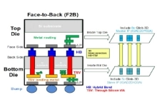
- GUC provides 3DIC ASIC total service package to AI/HPC/Networking customers
- DVB-S2X Wideband LDPC/ BCH Decoder IP Core Available For Integration From Global IP Core
- Cadence Announces Most Comprehensive True Hybrid Cloud Solution to Provide Seamless Data Access and Management
- Dolphin Design expands GoAsic partnership to enhance the semiconductor Industry's Supply Chain
- Cadence Collaborates with MemVerge to Increase Resiliency and Cost-Optimization of Long-Running High-Memory EDA Jobs on AWS Spot Instances
Most Popular
- U.S. Subsidy for TSMC Has AI Chips, Tech Leadership in Sight
- Cadence Unveils Palladium Z3 and Protium X3 Systems to Usher in a New Era of Accelerated Verification, Software Development and Digital Twins
- Zhuhai Chuangfeixin: OTP IP Based on 90nm CMOS Image Sensor Process Technology Successfully Mass Production
- Silvaco Announces Expanded Partnership with Micron Technology
- OPENEDGES Unveils ENLIGHT Pro: A High-Performance NPU IP Quadrupling its Previous Generation's Performance
|
|
E-mail This Article |
|
Printer-Friendly Page |