32-Bit RISC-V Embedded Processor and Subsystem, Maps ARM M-0 to M-4. Optimal PPA,


Tool Talk: Will 3D chips challenge SoCs?
 | |
| EE Times: Latest News How 3-D stacks up against SoCs | |
| Richard Goering (05/03/2004 2:00 PM EDT) URL: http://www.eetimes.com/showArticle.jhtml?articleID=19400243 | |
| � | |
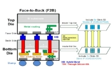
| A session on 3-D ICs at the recent International Symposium on Physical Design (ISPD2004) brought home a point worth remembering: Systems-on-chip don't represent the only path to higher functionality. There are other options, such as vertical stacks of multiple dice. There are many advantages to building chips "up" rather than "out," according to ISPD presenters. Making an analogy to Manhattan skyscrapers, IBM's Robert Montoye noted that with cities and ICs alike, the fastest way to add bandwidth is to go up. There are various ways to do that with ICs, ranging from two dice stacked into a single package to truly 3-D, multilayer "vertical VLSI" packages that operate like a single piece of silicon. Going vertical, as opposed to across chips, means shorter interconnects, less power and more speed. Three-dimensional schemes can produce huge bandwidth advantages, according to Montoye. "We need more storage and more capacity, and we need to get off the main die because it's too expensive to put it on the main die," he said. Rafael Reif, professor of electrical engineering at the Massachusetts Institute of Technology (MIT), made an interesting point as he presented MIT's work with 3-D ICs. Why cram analog and digital circuits onto a single die and then wrestle with signal isolation? Why not, instead, put separate analog and digital "layers" in a vertical 3-D stack? One limiting factor for 3-D chips is a lack of EDA tools. MIT developed its own tools for 3-D placement and routing, design rule checking and layout management. There are still problems to resolve with 3-D chips, such as heat removal. There may be practical issues that make them unfeasible. But they do raise an interesting question: Are we so accustomed to thinking about chip design in two dimensions that we've ignored something obvious? The real message to the EDA community is that systems-on-chip, as envisioned, aren't the only game in town. It would be a mistake to assume that designers will put all their functionality on one die just because the process technology theoretically allows it. There may be better, faster and cheaper ways to get complicated systems out the door. EDA vendors should weigh the options and not put all their eggs in the SoC basket. Richard Goering is managing editor of Design Automation for EE Times.
| |
| All material on this site Copyright � 2005 CMP Media LLC. All rights reserved. Privacy Statement | Your California Privacy Rights | Terms of Service | |
| � | |


Related News
- What’s the cost for 3-D chips?
- Chiplet Interconnect Pioneer Eliyan Closes $60 Million Series B Funding Round, Co-led by Samsung Catalyst Fund and Tiger Global Management to Address Most Pressing Challenge in Development of Generative AI Chips
- ARM pushes chiplets and 3D packaging for Neoverse chips
- Samsung Foundry Certifies Cadence System Analysis and Advanced Packaging Design Tool Flow for 2.5/3D Chip Designs
- ARC: from 3D Game Chips to Licensable RISC Processor
Breaking News
- Silicon Creations Reaches Milestone of 10 Million Wafers in Production with TSMC
- Analog Bits to Demonstrate Numerous Test Chips Including Portfolio of Power Management and Embedded Clocking and High Accuracy Sensor IP in TSMC N3P Process at TSMC 2024 North America Technology Symposium
- T2M-IP Unveils Revolutionary MIPI D-PHY & DSI Controller IP Cores with speed 2.5Gbps/lane, Redefining High-Speed Data Transfer and Display Interfaces
- Omni Design Technologies Joins Intel Foundry Accelerator IP Alliance
- Efabless Announces the Release of the OpenLane 2 Development Platform, Transforming Custom Silicon Design Flows
Most Popular
- GUC provides 3DIC ASIC total service package to AI/HPC/Networking customers
- Omni Design Technologies Joins Intel Foundry Accelerator IP Alliance
- Faraday Partners with Arm to Innovate AI-driven Vehicle ASICs
- Semiconductor Capacity Is Up, But Mind the Talent Gap
- Efabless Announces the Release of the OpenLane 2 Development Platform, Transforming Custom Silicon Design Flows
|
|
E-mail This Article |
|
Printer-Friendly Page |