
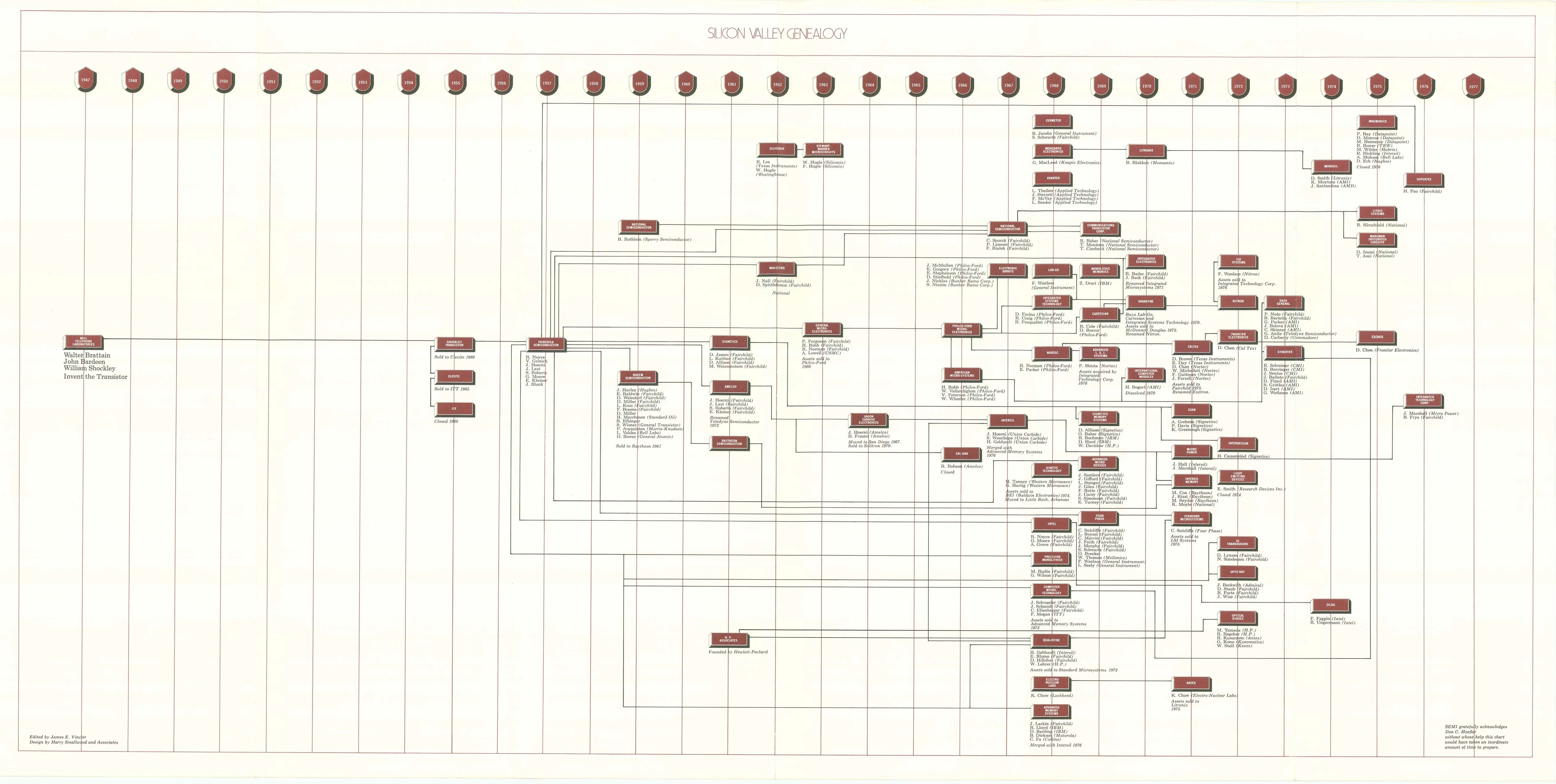
In the first 20 years of the industry, giants like Intel, National, and AMD were borne from Fairchild and built around the IDM (independent device manufacturer) model with each company owning its own fab. These companies went on to spin out their own innovators into successful companies as shown in this nifty graphic.
The next 20 years, starting around 1984, we saw yet another explosion of innovation in the semiconductor industry with the advent of the fabless model. It was here we started to see the “disaggregation” of the industry dramatically lowering the barrier to entry for entrepreneurs by allowing them to build a semiconductor company without having to own the fab. Here the likes of Broadcom, Xilinx, Marvell, Qualcomm come into existence and dominate through rapid innovation on the technology and design side, instead of the manufacturing side. All was right with the world—everyone was making money.
Cycle forward to 2001, where the crash of the Internet bubble brought to the semiconductor industry the longest and deepest recession in its history to that date. The result of this event was an industry that was dramatically leaner and more efficient. Innovation would now rely on a combination of internal development of technology (so-called organic growth) and inorganic growth through the acquisition of new technology from smaller companies. These smaller companies found their way into existence from a healthy supply of venture capital successes gained from the go-go days of the 80’s and 90’s.
However, by the end of the decade there were signs of trouble for entrepreneurs trying to get their new company off the ground. There were a number of factors at play here:
• It had become much more expensive to start a semiconductor company. In the early 1990’s, a new company could get off the ground for as little as $1M. By 2010, it was at least $50M to get the first chip. On top of that, there was still market risk (will people buy it? Are we too early, too late?), and the technology risk (will the chip work?).
• VC’s weren’t seeing the exit valuations that they once saw. The risk/reward was no longer balanced, especially with the increased capital demand.
• VC’s had plenty of other opportunities to put their money to work. Social networking, software, and other less capital intensive investments simply made more sense from an investment point of view.
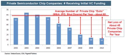
At the Global Semiconductor Alliance’s (GSA) Semiconductor Ecosystem Summit last October, a panel of investors presented interesting data on the state of new semiconductor startups, with this chart showing a dramatic decline in the funding on new semiconductor companies in the 2nd half of the 2000’s.
A continuous theme of the panel was that the semiconductor industry might be facing an innovation crisis, where there simply was no longer a rich supply of small innovative companies available for larger companies to acquire. However, a new meme arrived on the scene: a “Capital Lite” funding model that provides a new way to allow entrepreneurs to get their ideas out of the garage and into the market.
Based on a framework set out in an exciting paper by industry veterans Amer Haider (Cavium) and Awais Nemat (Marvell), the GSA struck out to assemble a working group of semiconductor professionals tasked with the mission of organizing a coalition of companies in the semiconductor supply chain to work with entrepreneurs to get their ideas off the ground.
To that end, a resource portal was established to pull all these companies together into a single place. Entrepreneurs can log into the portal and be connected with companies from the entire supply chain: EDA, IP, Foundry, Services, and even VC and other strategic investors from large semiconductor companies that will work with them to reduce the cost to get their chip to market under a model that is less risky to all involved. A new White Paper is available by clicking on the home page of the portal that describes the Capital Lite initiative in great detail and is a must read for all semiconductor professionals.
It is these types of initiatives that continue to make it exciting to work in Silicon Valley, the greatest place on earth for semiconductors more than 50 years after it all started back with Fairchild. I think that initiatives like this show that the semiconductor industry truly has grown up and is entering a new stage by recognizing that it must water its garden today to ensure the green sprouts of innovation will grow into the mighty oaks of tomorrow.
Warren Savage, President and CEO of IPextreme,is a well-known and published authority in the field of semiconductor intellectual property.
He has a long history of pushing the envelope of design methodology from his work in fault tolerant computing at Tandem Computers in the 1980’s and driving reliable design methodologies into commercial practice at Synopsys for its DesignWare IP product in the 1990s. Much of his thinking became embodied in the seminal book on IP reuse, the Reuse Methodology Manual.