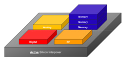
 One of the open areas for 3D chip design is what the design methodology needs to be and what design tools will be required. A more fundamental issue is going to be the business model to pay for tool development. At least in the short term, only a few 3D designs are going to be done and so a conventional EDA “build the tools and wait for everyone to do 3D designs” is not going to work. In fact Antun Domic of Synopsys, presenting at the 3D conference, explicitly pointed this out: EDA works economically when a large number of people use the same methodology so that the methodology can be wrapped up in the tools and sold in volume. Wally Rhines at the EDAC CEO forecast meeting said the same thing: that if semiconductor vendors expected to get 3D tools without paying incrementally for them then it was unlikely to happen.
IBM didn’t really talk about the design tools needed to design their 3D server chip with the processor on top and the memory underneath. But clearly designing a huge DRAM with holes for TSVs punched through it all over the place and the interconnect full of decoupling capacitors wasn’t done by hand.
One talk was by Vassilios Gerousis from Cadence and Damien Riquet from ST (calling in from France at 2 in the morning his time) about a 2.5D chip they had designed. They were using conventional Cadence tools somewhat unconventionally to get the job done, since it appeared there was no real explicit 3D support .
The first challenge in 3D design is to be able to analyze different approaches for efficiency: routing congestion, TSV density, microbump density, impact on power supply (IR drop etc). Unfortunately this is not straightforward since there are not yet any tools that do this directly: multi-floor floorplanners. The next best is to build the design and be able to analyze it. At this point in the technology there is not a lot of flexibility about what goes on what die since usually the die are different processes (DRAM, analog, RF, CCD etc). But eventually when designs stack multiple die and blocks of IP have several layers where they might reside then automation will presumably be required here just as floorplanning has become essential for regular 2D design.
 Cadence/ST created a tool to place the TSVs and the microbumps in regular arrays. Experience has shown that this tends to work better than putting them down randomly since you have some flexibility to design blocks with holes that have more than one place they can be located. They seemed to use a mixture of IC routing and custom design tools to design the interposer. They could then use conventional analysis tools and look at the system as whole from the point of view of power-supply analysis, static timing, thermal effects and so on. OpenAccess served as the link between the various tools, in particular allowing both digital tools (P&R) and custom tools (layout) to work on the same data.
I think the most interesting thing about this is that, at least for a relatively simple design with a non-active silicon interposer, it was possible to get the design done without requiring a complete portfolio of new tools with new support.
The biggest areas of opportunity (and biggest may be a relative term since it is not clear how big the market is for any of these) are floorplanning and general validation of the design (do all microbumps line up, are the voltage levels between die OK and so on). All the big EDA companies have some sort of place & route and floorplanning and might decide to play here. Then there is thermal analysis where a company like Gradient probably has an opportunity to extend their technology into another dimension. General analysis of the electrical aspects of the design could be an opportunity for Apache. Right now the biggest risk for an EDA company is likely to be over-investment rather than missing the boat. 3D ICs are coming but there is not going to be an instantaneous switch with thousands of 3D design starts any time soon, if ever.
