Consistent with the thoughts I’ve written about in this column over the last few years, John described the genesis of EDA 360 as being driven by the disruptive nature of Apple’s iPhone. That product- more than any other in modern history, has changed the rules of the game for everyone in the electronics business. John went even further stating “That device changed and will continue to impact and change every consumer device that gets built” and the expectation by the users of those devices who can personalize them to their own needs has “forever changed and will never go back.”
But the question is what’s the EDA 360 vision got to do with Cadence and why is this man so excited about it?
To understand that, we need first to summarize some of the key tenets of the EDA 360 vision with respect to the role of EDA in the semiconductor industry. EDA has historically existed to provide tools to help engineers keep up with the breakneck pace of Moore’s law. Improvements in efficiency largely revolved around “design creation”, or in other words helping engineers create more designs, faster, and with better quality. However, what we see today are not any breakthroughs in how engineers design as we saw in the nascent days of EDA some 25 years ago, but rather small, continuous improvements to existing point tools amid an ever shrinking number of design starts into which to sell these tools.
Going forward, John believes there needs to be a shift in the mindset of the EDA industry to recognize the reality that there are fewer “design creators” and more “design integrators” in building modern SoC devices. Just as the iPhone platform gave rise to an entirely new ecosystem of application developers to support a massive user community, EDA needs to retool to support semiconductor companies to quickly and efficiently produce products that can support this new paradigm of configurable, customisable hardware and software.
I noted to John that this was all well and good, but what is Cadence doing in response to this vision? He reminded me of the main pillars of EDA 360:
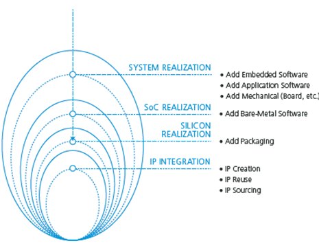
• Systems Realization
• SoC Realization
• Silicon Realization
• IP Integration
 He then went on to say that Cadence has changed the way they think about every aspect of their business as it relates to the vision. It has affected product roadmaps, the focus areas for R&D, and even produced reorganizations to remove any structural impediments to realizing the vision.
While this all sounds very good, it seems that the EDA industry of today is quite far away from the one described in EDA 360. I told John that while the vision sounds convincing at the theoretical level, are customers really willing to pay more if you do more? “That’s the $64,000 question.”, John said, “As an industry, we’ve given our value away. We did this to ourselves (competing on price). This is literally a market do-over. We have a chance to change the rules. There is going to have to be sanity in the market. We need to win by providing superior value.”
Turning to a subject near and dear to me, semiconductor IP, I asked John for his perspective on the IP market, which has continued to outpace the growth of both semiconductor and EDA markets over the last decade. John believes that the emergence of the IP market was a missed early indicator of the big changes afoot in the semiconductor industry that companies are just now coming to appreciate. As shown in a figure from the EDA 360 whitepaper (inset above), IP represents the core of modern semiconductor design.
The fact that IP is at the core of EDA 360 should come as no surprise. As larger and larger SoC devices are produced, the quantity of purchased 3rd-party IP contained in them is exploding and companies are relying on an increasingly diverse set of suppliers, including EDA companies. Synopsys pioneered IP in the EDA market with the launch of DesignWare nearly 20 years ago. Mentor Graphics followed some years later with its Inventra line while Cadence until recently kept a low profile in the IP area, confining its IP efforts to those with services component, perhaps a vestige of its pre-Tality days. John believes that Cadence’s delayed splash into the IP market until recently with the acquisition of Denali was wise. John notes that “quality is the imperative in IP” and a lot early providers have been shaken out by the market and that Cadence has benefited from being a late-mover by being able to enter that market through acquisition of proven players.
I closed our discussion with a very pointed question: “John, I’ve heard people say EDA 360 is just a Cadence thing. Is that fair rap?” John put it this way. Cadence takes the EDA 360 vision very seriously and believes that it’s essential to get the EDA industry realigned around the changing problems that their semiconductor customers are facing. They spent considerable time creating that vision that reflects not just what is good for Cadence but what’s good for the whole electronics industry. Most importantly, they see this as a time for an industry that isn’t growing to rally around solving customer problems as the antidote for slow growth. John noted that he has seen his competitors speak at public events and saw them using the same words as he does and promoting the same sort of worldview. They don’t call it EDA 360, but that’s just fine for John.
Warren Savage, President and CEO of IPextreme,is a well-knownand published authority in the field ofsemiconductor intellectu alproperty.
He has a long history of pushing the envelope of designmethodologyfrom his work in fault tolerant computing at TandemComputers inthe 1980’s and driving reliable design methodologiesintocommercial practice at Synopsys for its DesignWare IP productinthe 1990s. Much of his thinking became embodied in the seminalbookon IP reuse, the Reuse Methodology Manual.