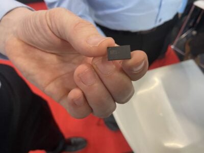
5nm nanosheet transistors cut power by 75%
Instead of using FinFET structures, engineers at the IBM-led Research Alliance at the SUNY Polytechnic Institute Colleges of Nanoscale Science and Engineering’s NanoTech Complex in Albany, NY, used a ‘gate-all-around’ (GAA) built with silicon nanosheets. For the last ten years IBM has been working on nanosheets where each 2D layer is one atom thick and stacked layers build up the structure of the transistor.
This enabled the first practical use of extreme UV (EUV) process technology at research partner GLOBAL FOUNDRIES as the nanosheets can be more easily aligned to build up the devices. This provides a 40% performance boost at fixed power over current 10nm FinFET devices, or a 75% power saving for the same performance.
Using EUV lithography, the width of the nanosheets can be adjusted continuously, all within a single manufacturing process or chip design. This adjustability permits the fine-tuning of performance and power for specific circuits – something not possible with today’s FinFET transistor architecture production, which is limited by its current-carrying fin height. Therefore, while FinFET chips can scale to 5nm, simply reducing the amount of space between fins does not provide increased current flow for additional performance.
The silicon nanosheet transistor is described in the Research Alliance paper Stacked Nanosheet Gate-All-Around Transistor to Enable Scaling Beyond FinFET, and published by VLSI.
“As we make progress toward commercializing 7nm in 2018 at our Fab 8 manufacturing facility, we are actively pursuing next-generation technologies at 5nm and beyond to maintain technology leadership and enable our customers to produce a smaller, faster, and more cost efficient generation of semiconductors,” said Gary Patton, CTO and Head of Worldwide R&D at GLOBALFOUNDRIES.
The same Extreme Ultraviolet (EUV) lithography approach was used to produce a 7nm test device with 20 billion FinFET transistors. The GAA nanosheet transistor architecture at 5nm would put 30bn transistors on a chip.
“We believe that enabling the first 5nm transistor is a significant milestone for the entire semiconductor industry as we continue to push beyond the limitations of our current capabilities,” said Dr Bahgat Sammakia, Interim President of the SUNY Polytechnic Institute.
 If you enjoyed this article, you will like the following ones: don't miss them by subscribing to :
eeNews on Google News


