Synopsys Cloud
Cloud native EDA tools & pre-optimized hardware platforms
Request a Free Trial →
In this era of revolutionary technologies, memory plays a vital role in any application that requires high-speed processing. High-resolution graphics require high-speed and high-bandwidth graphics memory, resulting in rapid adoption of next generation memory technology High-Bandwidth Memory (HBM). HBM is finding its way into leading-edge graphics, networking, HPC (High Performance Computing), and Artificial Intelligence systems; for example, decoders for a video signal, fully autonomous vehicles, neural network designs, and other advanced applications that demand low power and massive bandwidth. Our previous memory blog – Next generation memory technologies: Ready to take the verification challenges?, discussed several next generation memory technologies across applications. This blog will review the details of HBM, a next generation memory technology for graphics, networking and HPC.
Over the past decade GDDR5 has been an industry standard and has reserved a prominent place in all graphics oriented technologies. GDDR5 is focused on using more power to achieve greater clock speeds. GDDR5 chips are attached directly to the graphics card in a single layer, which means adding more memory involves spreading out horizontally on the graphics card. Power consumption and form factors have thus been major concerns. HBM has emerged as an alternative which breaks all processing bottlenecks.

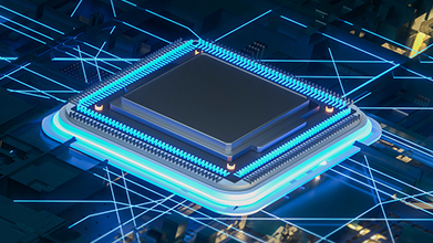
HBM is a 3D DRAM technology with stacks of up to eight DRAM dies, which are interconnected by TSV (Through-Silicon Vias), and microbumps. It is tightly coupled to the host compute die with a distributed interface. The interface is divided into completely independent channels and not necessarily synchronous to each other. The HBM DRAM uses a wide-interface architecture to achieve high-speed, low-power operation. HBM is now upgraded to HBM2 which specifies up to eight dies per stack and doubles pin transfer rates up to 2GT/s, making it useful for performance sensitive consumer applications.

Like any other DRAM, HBM memory is controlled by commands from the host memory controller. It provides two independent row and column command interfaces, allowing activates/precharges to be issued in parallel with read/writes and therefore this simplifies controller operations and increases efficiency. It processes 128 bits of data at a time and supports 2n prefetch architecture with 256 bits per memory read and write accesses.
One of the key enhancements of HBM2 is its pseudo channel mode, which divides a channel into two individual sub-channels of 64 bit I/O each. These channels are semi-independent. In legacy mode, each page has a size of 2KB but in pseudo channel mode, it’s only 1KB. The larger the page size, the larger the amount of power that’s needed to open a page. Since pseudo channel pages are only half the size, it also requires roughly half the current. These pseudo channels operate semi-independent, they share the channel’s row and column command bus as well as CK and CKE inputs, but decode and execute commands individually. They also share the device mode registers.
HBM also features a temperature sensor, which can be read by the controller to adjust its refresh rate. It supports temperature compensated self-refresh. RAS (Reliability, Availability, and Sensitivity) features include support for ECC (Error Correction code) for data error correction and column/row address/data parity checking. Another attractive feature of HBM is its JTAG connectivity for IEEE-1500 access, AWORD and DWORD training, lane repair, boundary scanning and loopback test modes. These built-in self-test (BIST) and built-in self-repair (BISR) features make HBM one of the most sophisticated dynamic RAMs. These test features are used in the final test steps of the assembled System in Package (SiP).
To conclude, HBM is a breakthrough memory solution for performance, power and form factor constrained systems, delivering high-bandwidth, low effective power and small form factor. Unlike conventional memory setups where DRAM chips are placed as close as possible to each other on a circuit board, HBM stacks a bunch of RAM dies on top of each other.
Stay tuned for upcoming blogs on emerging next generation HBM and other memory specifications, and detailed description of HBM features such as pseudo channel and IEEE testmode. Synopsys provides VIP for HBM2/HBM supporting complete protocol including the IEEE test mode, along with run time configurable timing parameters, extensive timing and data integrity checks, Verdi protocol and performance analyzer. For more information on Synopsys memory VIP and Test Suite, please visit http://synopsys.com/vip.