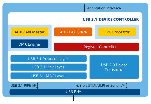
USB 3.1 Device controller is a highly configurable core and implements the USB 3.1 Device functionality that can be interfaced with third party USB 3.1 PHY’s. USB3.1 Device controller core is part of USB3.0 family. This Device Controller core is architected with an high performance DMA engine based on USB3.1 specification.
This Controller core is carefully partitioned to support standard power management schemes which include extensive clock gating and multiple power wells for aggressive power savings required for mobile and handheld applications. This controller has a very simple application interface which can be easily adapted to standard on-chip-bus interfaces such as AXI, AHB, OCP as well as other standard off-chip interconnects making it easy to be integrated in a wide range of applications. The Controller also has a dedicated PHY Type-C connector Interface for identifying Type-C specific features such as cable orientation, ID function based on Configuration data channel etc.
Design is highly modular and configurable, offering versatility in customization.
Embraces a layered architecture for streamlined development and scalability.
Operates on a fully synchronous basis, ensuring precise timing across all components.
Supports both synchronous and asynchronous reset functionalities for flexible operation.
Features clearly defined clock domains, enhancing system stability and performance.
Provides extensive support for clock gating, optimizing power consumption.
Offers multiple power well support, enabling efficient power management.
Key features are controllable via software, allowing for convenient management and customization.
Customizable RTL Design
HDL-based Test Bench with Behavioral Models
Test Case Suite
Protocol Compliance Validators, Bus Observers, and Performance Trackers
Configurable Synthesis Framework
Design Manual
Verification Handbook
Synthesis Procedure Guide
FPGA Validation Platform for Pre-Tape-out Testing
Reference Firmware Implementation
