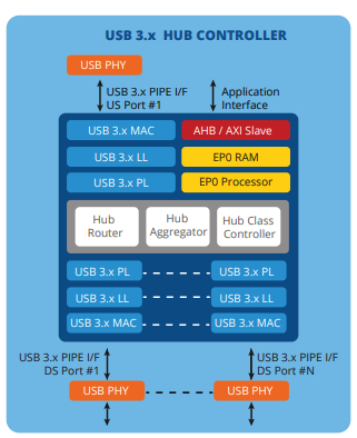
USB 3.1 Hub controller is a highly configurable core and implements the USB 3.1 Hub functionality that can be interfaced with third party USB 3.1PHY’s. USB3.1 Hub controller core is part of USB3.0 family of cores.The core leverages GDA’s design expertise from its high speed interconnect family of IP’s including PCI Express, Serial Rapid IO and Hypertransport.
This Hub Controller core can be configured to support upto 15 downstream ports. This Hub Controller core supports all defined USB 3.1 power states. The design is carefully partitioned to support standard power management schemes. Optionally, it can be configured to manage power mode transitions of the controller and the USB 3.1 PHY for aggressive power savings required for bus powered hubs. The controller's simple, configurable and layered architecture is independent of application logic, PHY designs, implementation tools and, most importantly, the target technology.
Features a highly adaptable and customizable design, catering to diverse configurations and requirements.
Utilizes a layered architecture to enable structured development and scalable deployments.
Ensures precise coordination through full synchronicity in operation.
Offers flexible reset options with support for both synchronous and asynchronous resets.
Facilitates clear system delineation with well-defined clock domains.
Optimizes power usage through robust clock gating mechanisms.
Enables nuanced power management with support for multiple power wells.
Provides software-controlled access to essential features, enhancing system manageability and customization options.
Customizable RTL Design
HDL-based Test Bench with Behavioral Models
Test Scenario Suite
Protocol Verification Tools, Bus Monitors, and Performance Analyzers
Configurable Synthesis Framework
Design Reference Guide
Verification Handbook
Synthesis Procedure Manual
FPGA Validation Platform for Pre-Tape-out Testing
Firmware Code Reference
