Arm Moves Production-Level EDA to the Cloud with the Help of AWS

By Rene Haas, President, IPG, Arm
News highlights:
- Migrating design and verification to Amazon Web Services (AWS) Graviton2 instances reduces cost, complexity and risks, while increasing throughput by up to 10x
- Cadence, Mentor, Synopsys and other leading EDA vendors are porting and optimizing their technology to run on Arm compute environments
- An Arm-based environment for designing Arm-based silicon in the cloud will accelerate innovation and choice for everyone in the ecosystem
Released in February, the Arm Cortex-M55 CPU quickly became a milestone for the Arm ecosystem because it gave hardware and software developers the power to incorporate unprecedented ML capabilities into the billions of IoT products coming to market. It also was the first time Arm leveraged Arm-based AWS Graviton2 instances to perform production-level design validation for its IP.
As AWS announced last week, Arm is moving the majority of its Electronic Design Automation (EDA) workloads to AWS, as part of our effort to reduce our global datacenter footprint by at least 45% and our on-premises compute capabilities by 80% as we complete our migration to AWS.
We have already realized a 6x improvement in performance time for EDA workflows on AWS and see the potential for increasing throughput by 10x. In addition, Arm is generating powerful engineering, business, and operational insights that help increase workflow efficiency and optimize costs and resources across the company.
Our goal ultimately is to move most of our design work to Arm-based cloud services over the next several years, and we think we will have company too. By sharing our experiences across the Arm ecosystem, we hope to encourage partners to design their Arm-based silicon on Arm-based cloud services.
EDA: An Inside Job Until Now
EDA in many ways is a natural fit for the cloud as chip designers often need simultaneous access to tens of thousands of CPUs to run this compute-intensive task. Meeting tight deadlines can mean consuming millions of core-hours per month. Building a data center to accommodate the gigantic bursts of computing power needed for tomorrow’s complex devices is well beyond the reach of most organizations.
Most EDA workloads, however, still largely get performed in on-premises data centers owned and/or managed by semiconductor companies because of the complexities and risks involved in migration. Importantly, design workflows have to be unified and semiconductor designers have to figure out a balance between workloads that are best suited for cloud, and which make more sense staying in-house.
To bridge this chasm, Arm has been working with major EDA partners such as Cadence Design Systems, Mentor Graphics’ (a Siemens Business), and Synopsys to port their EDA tools to Arm. Already we’re seeing significant results in terms of performance and cost savings for customers.
Likewise, AWS continues to expand its portfolio to accommodate these types of workloads. The recently unveiled AWS Graviton 2-based C6gn instance delivers up to 100 Gbps networking while providing a 40% price-performance advantage over conventional processors.
An Arm-on-Arm World
Arm certainly won’t be alone in looking at ways to improve the semiconductor industry through the cloud. The Fifth Wave of computing (the convergence of 5G, AI, and IoT) provides the technology community with an unprecedented opportunity to make a difference in the world. Autonomous cars will reduce accidents and emissions, while track and trace technologies will help contain COVID-19. Silicon will continue to get smarter and will be even more omnipresent in our lives.
Ubiquitous computing, however, will also mean developing products that are smaller, smarter, more distinct in their design, and less expensive than ever before. We as an industry will also have to meet these seemingly contradictory goals in less time and with fewer dedicated resources. Design, simulation, and verification in the cloud—particularly on compute instances that can deliver maximum performance with minimum energy consumption—can erode the barriers that exist between an idea and a finished product produced in volume. Just as cloud services transformed the software business, new services and new startups will follow as cloud-based silicon design takes hold.
If you would like to learn more, please check out the expert blogs on our EDA in the cloud journey in the Arm Community.

Any re-use permitted for informational and non-commercial or personal use only.
Media Contacts
Latest on Twitter
Congratulations to Tamika Curry Smith, our Chief DEI Officer who has been chosen as one of @SavoyNetwork's Most Influential Executives in Corporate America for 2024. 👏
The honor recognizes Tamika's commitment to community, leadership, and success: https://okt.to/2NvDOZ
This #EarthDay, we're celebrating our collaboration with @UNICEF, to unlock the life-changing potential of technology in Malawi.💧
Our investment has helped UNICEF install two water supply systems, helping provide 11,000 people with access to safe water and sanitation services.

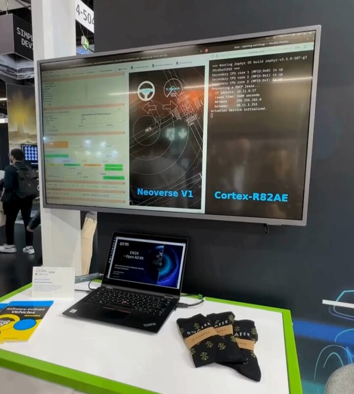
ISA parity is accelerating silicon and software deployment in automotive! 🚗💨
👇 At #ew24 we showcased what this looks like in practice via virtual platforms with our Neoverse-based cloud instances and new Arm AE IP, which brings almost 100% ISA parity. https://okt.to/cjVaFN
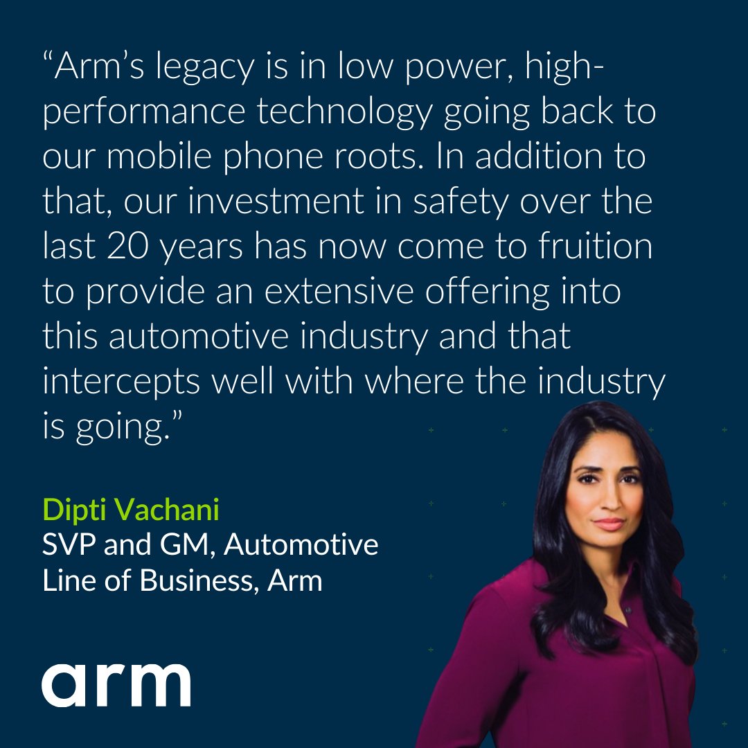
The future of automotive is here. 🚀
Hear from Dipti Vachani on @IBDinvestors as she shares details on the game-changing performance and functional safety features of our new Armv9-based AE processors and server-class Neoverse technology: https://okt.to/WVtw58
AI is expected to increase data center power consumption 3️⃣x by 2030.
To offset this, hyperscalers like Amazon and Google turn to Arm Neoverse to reduce power without compromising performance.
That's why the future of AI is built #onArm. https://okt.to/LPVFWd
We're working with our partners @Simprints, @Gavi and @_GHSofficial to enable healthcare equity in Ghana.
Built #onArm, Simprints technology is enabling vaccine equity by making it easier to verify vaccine delivery by individual: https://okt.to/MIcgxu

If Arm technology is in there, then the future will be too.
Our energy-efficient compute platforms are foundational to the world's technology and AI computing, shaping how we work, play and connect.
That's why the future is built #onArm. https://okt.to/M9wqc8

Here's to a fantastic week at Embedded World! 🎉
From lightning talks and speaker sessions to demos of our latest automotive and IoT technologies, we brought our vast ecosystem together to showcase what's possible when you build #onArm.
Thank you to everyone that joined us. 👏


🚗 Software-defined vehicles (SDVs) are the future of automotive and they're being built #onArm.
Robert Day joins @Sonatus and @MotorTrend on the latest podcast to talk all things SDVs and where the industry is headed.
🔊👇 Listen below.
🏆 And the winner of the Embedded Awards 2024 goes to… @Ambiq_AI's Apollo510 MCU!
This winning tech opens the door to new local AI opportunities on billions of devices.
Listen in as the team talk us through their exceptionally efficient Arm-based SoCs at #EmbeddedWorld.

David Maidment recently shared his thoughts on the future of edge computing at #EmbeddedWorld!
Missed the talk? Catch up on his insights into the evolution of edge computing across billions of diverse connected devices to build a secure AI-enabled future: https://okt.to/EtfSRN


AI is everywhere at this year's #EmbeddedWorld.
🚘 With the demand for more autonomy, increasingly advanced user experiences and the trend toward electrification Dennis Laudick shares why AI will remain crucial to drive innovation in the software-defined vehicle.
#ew24

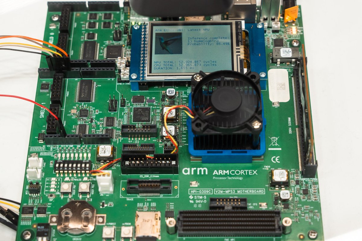
Two identical demos. One different NPU.
Our new Ethos-U85 NPU is optimized for transformer networks to deliver the performance needed for edge AI use cases - including high performance voice and vision experiences.
This makes it perfect for AI applications like Gen AI. #ew24

We're ready for the final day of #EmbeddedWorld! 🚀
It's been a fantastic show so far showcasing our power-efficient compute platforms that are fueling the future of edge AI.
Reply with an emoji to let us know if you'll be visiting us on the show floor. 👋
#ew24


What's trending at #EmbeddedWorld?
AI, AI and more AI. 🔥
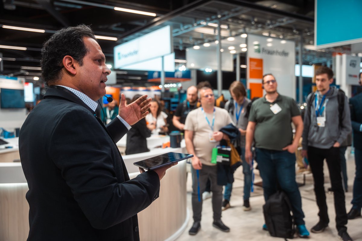
@pnwilliamson shares where you might find edge AI in action from our ecosystem partners building the future #onArm. #ew24

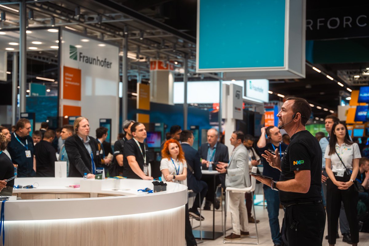
At the Arm booth at #EmbeddedWorld you'll find:
✅ Partner demos from the likes of @NXP, @Ambiq_AI and @_Elektrobit
✅ Partner Lightning Talks from @Microsoft, @EdgeImpulse and more
✅ Our latest IoT and Automotive tech
#ew24

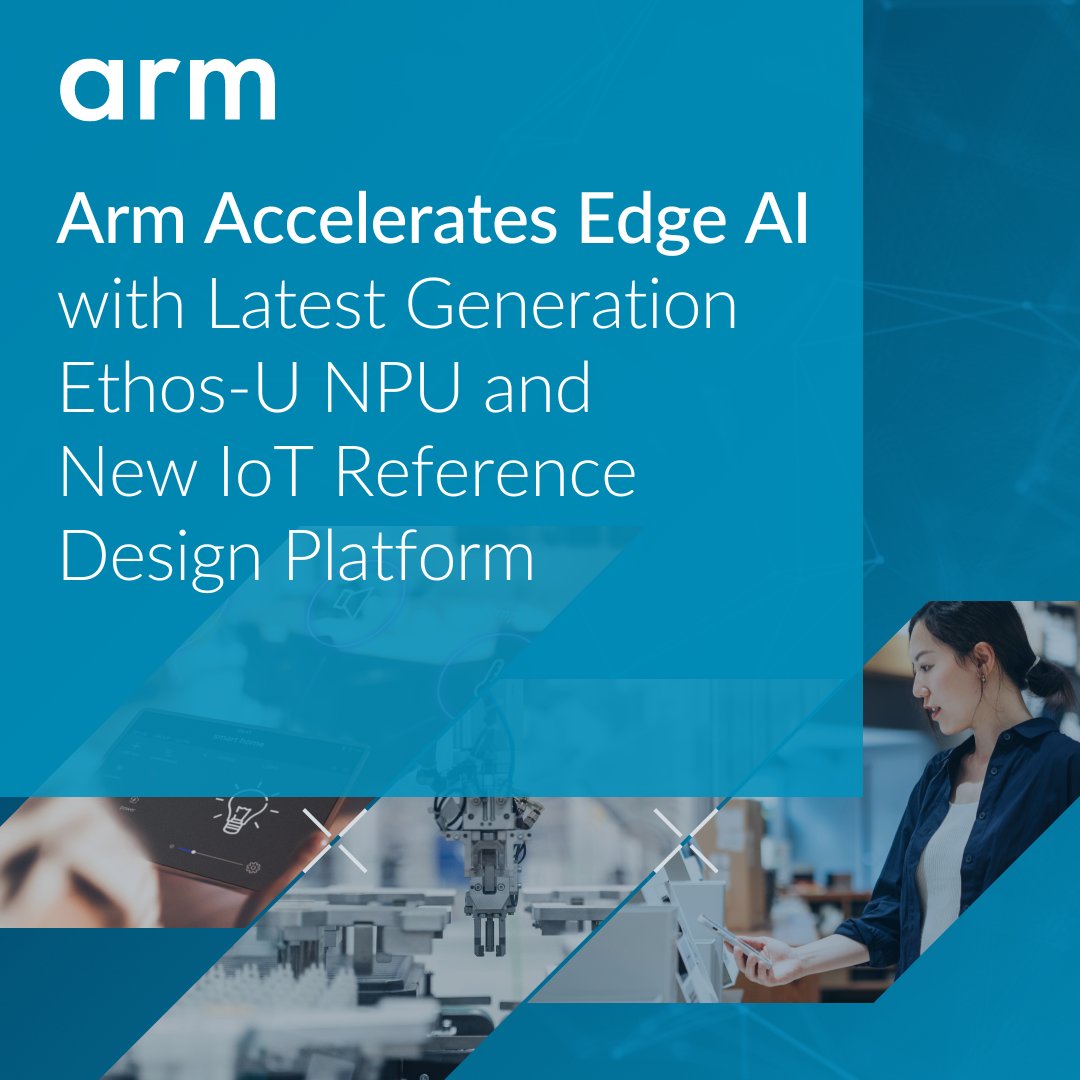
🚀 We're taking edge AI innovation to the next level with the new Arm Ethos-U85 NPU and Corstone-320 IoT Reference Design Platform.
@pnwilliamson shares how these new technologies are transforming future voice, audio and vision applications live from #EmbeddedWorld. #ew24

Get to know LaunchX from NetsPresso by @nota_ai, on show at #EmbeddedWorld. 👇
Designed to help you easily convert and benchmark AI models, it supports a ton of Arm-based devices from our partners including Arduino, NXP, Renesas, Raspberry Pi and NVIDIA. #ew24

🇺🇸🇯🇵 We're proud to support new AI research partnerships between universities in the US and Japan.
Through close collaboration between business, academia and government we can continue to advance AI innovation to transform industries and improve lives. https://okt.to/9JbahF


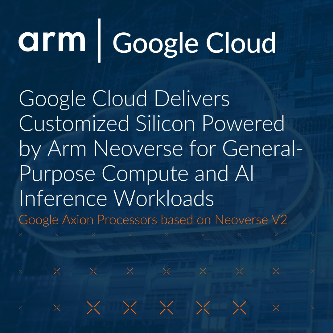
📢 Custom Arm-based silicon from @GoogleCloud is here!
Axion, built on Armv9 Neoverse V2, will bring performance & energy efficiency gains to AI inferencing & general-purpose workloads, like web and app servers.
Congrats to the team! 👏 https://okt.to/xS4cBN #GoogleCloudNext
It's time for #EmbeddedWorld! 🙌
We're in Nuremberg this week showing you how to build your AI-accelerated future #onArm. 🎉
Can’t join us in person? Keep up to date on social media for live updates from the show! #ew24

🆕 Get ready to accelerate edge AI with the new Arm Ethos-U85 NPU and Corstone-320 IoT Reference Design Platform. ⚡
With performance and efficiency uplifts, developers can now deliver greater AI compute in smaller, more cost-sensitive devices: https://okt.to/cJPTCQ
When it comes to AI and ML at the edge, challenges like hardware fragmentation and performance optimization stand in the way of widespread adoption.
@pnwilliamson shares how developers can navigate this, with an invitation to join us at Embedded World: https://okt.to/tpsPTd

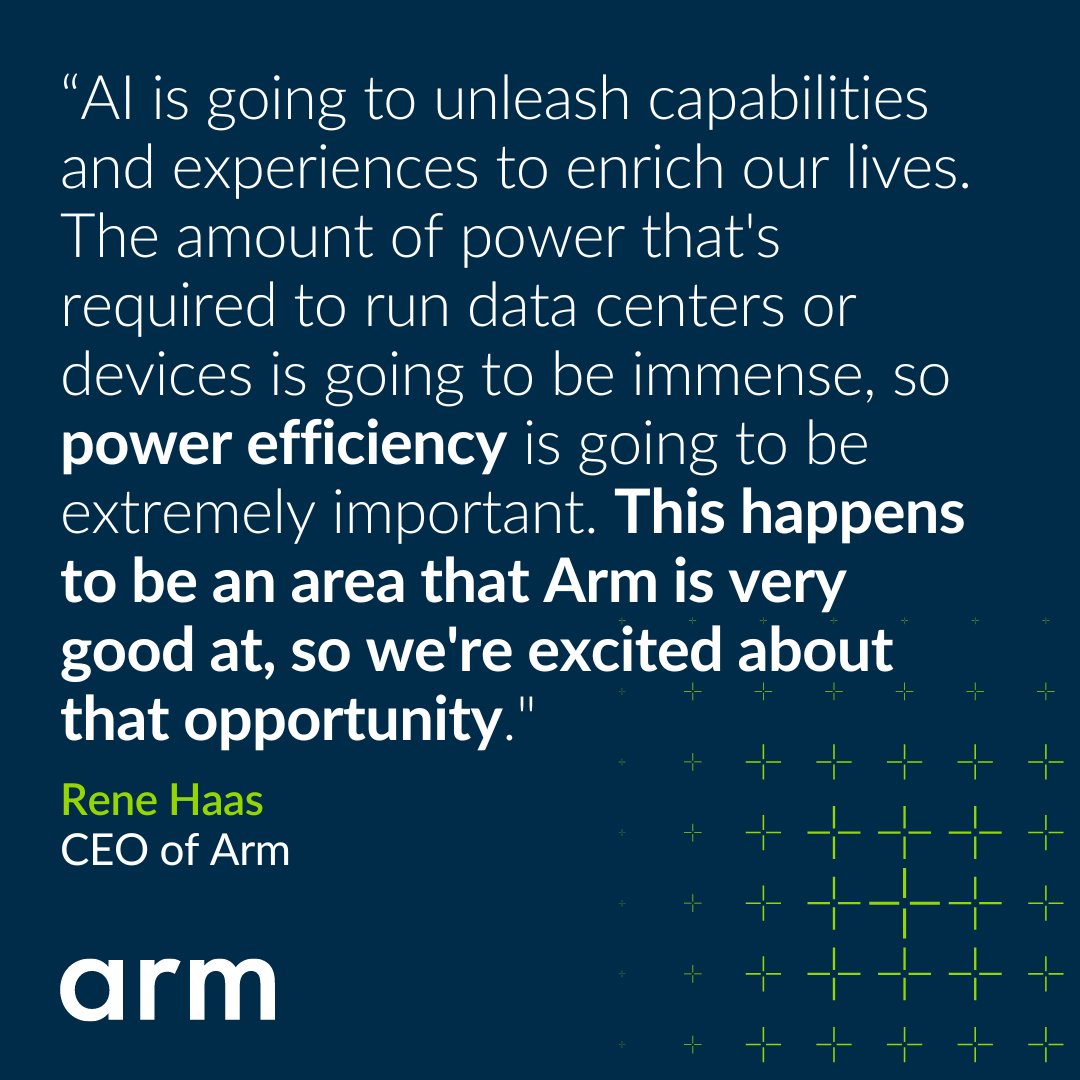
With the AI boom fueling demand for compute, our CEO Rene Haas speaks to @jchatterleyCNN on the importance of ecosystem collaboration to unlock unique capabilities we've not seen before.
Listen to the @CNN podcast at 28:38 for the full interview 👉 https://okt.to/mcH1tF