Description and Features
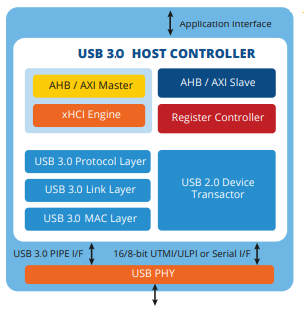
We provide highly configurable and scalable USB 3.1 host/device/dualmode controller IP Cores for a wide range of applications. The USB3.0 host controller is a highly integrated and cost-effective IP. It contains a USB3.0 PHY and a USB2.0 PHY. The USB3.0 PHY is used for Super-Speed (SS) transfers and the USB2.0 PHY is used for High-Speed (HS), Full-Speed (FS), and Low-Speed (LS) transfers. The USB 3.0 controller is designed for compliance with USB3.0 specification, Revision 1.0 and all associated ECNs, as well as USB specifications Rev 2.0 and associated ECNs. The USB 3.0 host controller based on xHCI specification, can be used in systems running any OS which provides xHCI/USB stacks, such as Android, Linux, or Windows. The USB 3.0 host controller exposes either an AXI or AHB master interface for the data path and an AHB slave interface for register access. Optionally, an interoperate proven third-party PCIe-AXI/AHB bridge can be provided for use in standard desktop/server applications.
Features
-
Compliant with XHCI Specification, Revision 1.0
-
Compliant with USB 2.0 Specification, Revision 2.0
-
Compliant with USB 3.0 Specification, Revision 1.0
-
Supports DFT test for digital parts of the controller
-
Supports Loopback test for USB2.0 PHY and USB3.0 PHY
-
Compliant with USB 2.0 specification, Revision 2.0
-
Supports High-Speed (480Mbps), Full-Speed (12Mbps) and Low-Speed (1.5Mbps) serial data rates
-
Embedded 45ohm High-Speed termination, 1.5kohm Full-Speed device pull-up resistor, 15kohm pull-down resistors
-
Embedded Phase-Locked Loop (PLL) for 480MHz High-Speed USB operations
-
Embedded internal RREF for reference current trimming function
-
Embedded HV protection circuit
-
Provides one 5Gbps Super-Speed connection
-
270MHz differential CMOS reference clock
-
0.9V/1.8V supply rails
-
On-chip 50Ω termination resistors
-
10-bit parallel interface (@ 500MHz)
-
Programmable transmitter output swing and de-emphasis strength
-
Configurable/adaptive equalizer to optimize receiver sensitivity
Benefits
-
Highly modular and configurable design
-
Layered architecture
-
Fully synchronous design
-
Support for both sync and async reset
-
Clearly demarcated clock domains
-
Extensive clock gating support
-
Multiple power well support
-
Software control for key features
Applications
-
Desktop / Server Applications
-
Automotive
-
Smartphones
-
Tablets
-
Notebooks
-
Gaming
-
Digital cameras and camcorders
-
Storage
-
Wireless communication
-
Set-top boxes
-
Smart TVs and digital TVs
-
Chip-to-chip low-power interconnects
Deliverables
-
Customizable RTL Design
-
HDL Test Bench with Behavioral Models
-
Test Case Repository
-
Protocol Compliance Validators, Bus Monitors, and Performance Analyzers
-
Configurable Synthesis Framework
-
Design Handbook
-
Verification Manual
-
Synthesis Procedure Guidebook
-
FPGA Validation Platform for Pre-Tape-out Verification
-
Firmware Reference Implementation and Documentation
