Description and Features
ONFI PHY block is used to either transmit signal and data to NAND Flash interface or receive the data from NAND Flash by Flash controller IP. MDLL sets the delay time for the control signal of PHY to access to the data in flash during the suitable period. Please refer to the following diagram for an overview of ONFI PHY.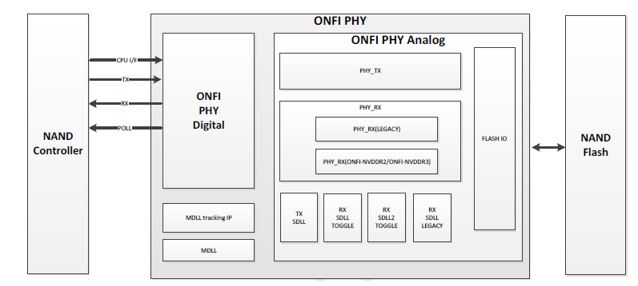
Features
-
Support ONFi 4.1 IO Electrical Specification
-
Support Legacy up to 50MHz
-
Support NV-DDR2 up to 533Mbps
-
Support NV-DDR3 up to 1200Mbps
-
Per DQ (per bit) delay line for controlling skew
-
SDLL is included for DQS/DQ phase tuning by DLY setting
-
On die De-coupling capacitor (>1nF per channel) for Power Integrity to save PKG capacitor
-
Operation temperature: -40 to 125 °C
-
Flip-Chip
-
Supported metal scheme:
-
1P9M_2Xa1Xd3Xe2Z
-
1P10M_2Xa1Xd4Xe2Z
