Description and Features
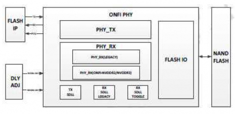
ONFI PHY block is used to either transmit signal and data to NAND Flash interface, or receive the data from NAND Flash by Flash controller IP. MDLL sets the delay time for the control signal of PHY to access to the data in flash during the suitable period. Please refer to the following diagram for an overview of ONFI PHY.
Features
-
Support ONFi 4.0 IO Electrical Specification
-
Support Legacy up to 50MHz
-
Support NV-DDR2 with operating frequency up to 533Mbps
-
Support NV-DDR3 with operating frequency up to 800Mbps
-
Per DQ (per bit) delay line for controlling skew
-
SDLL is included for DQS/DQ phase tuning by DLY setting
-
On die De-coupling capacitor (>1nF per channel) for Power Integrity to save PKG capacitor
-
Operation temperature: -40 to 125 °C
-
Programmable output impedance
-
TSMC 28nm HPCP 1P7M5X1R (HVT/LVT/EHVT) process
-
Wire-bond
Deliverables
-
Application Note / User Manual
-
Behavior model, and protected RTL codes
-
Protected Post layout netlist and Standard Delay Format (SDF)
-
Synopsys library (LIB)
-
Frame view (LEF)
-
Metal GDS (GDSII)
-
Test patterns and Test Documentation
Benefits
-
Silicon Proven in TSMC 28HPC+
-
In Production in multiple Chipsets
Applications
