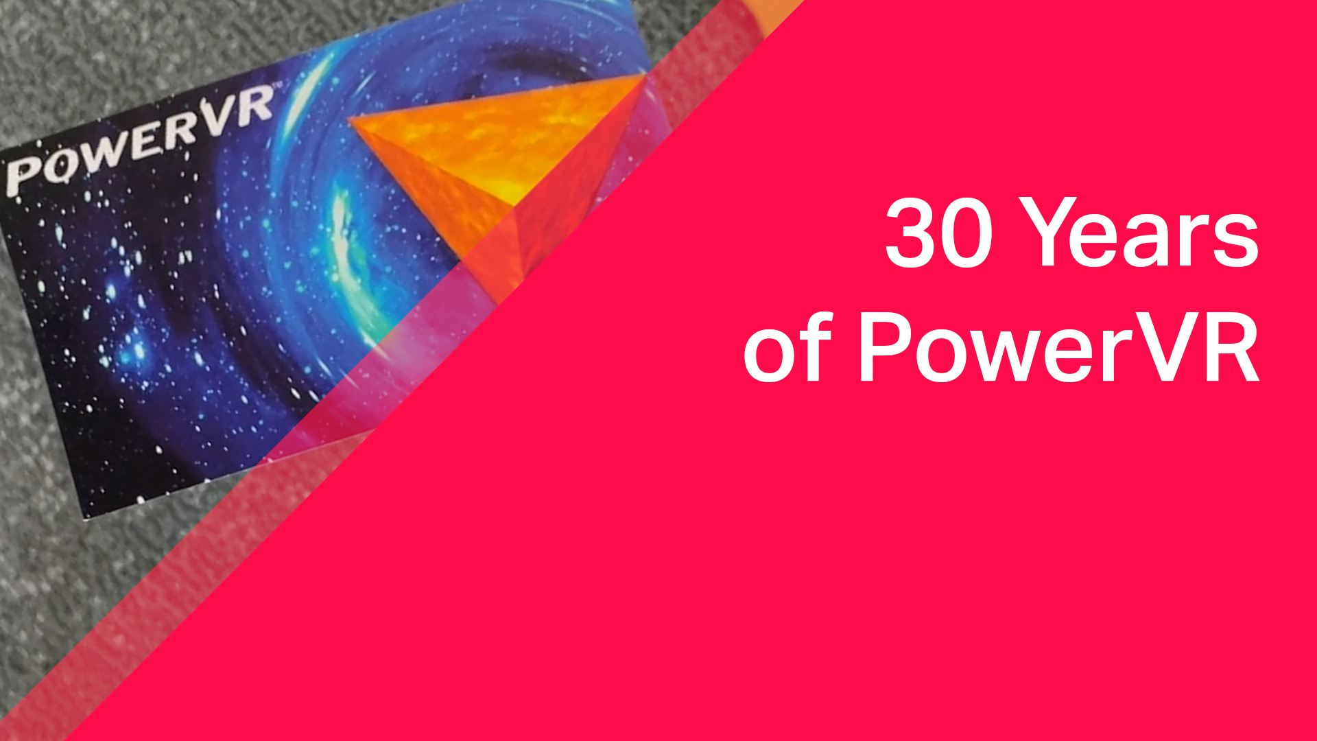
I was recently privileged to be asked to deliver a keynote on the semiconductor IP business to a distinguished group of engineers at the IEEE SoC Conference in Belfast. While I’m a lifelong marketing man rather than an engineer, hopefully, my 25 years working in the IP industry has enabled me to view it from all angles and offer up some insight. Let’s dive in…
The state of the market
In recent years, the semiconductor market has been characterised by several factors. These include increased demand, cyclical supply, constant technological change, price erosion, evolving standards and varying product life cycles. Periods of diminished product demand have led to downturns, resulting in erosion of average selling prices (ASPs) and other factors that impact customers and the markets in which they operate.
On the upside, an increased requirement for high-performance IP solutions has bolstered the technology market and, to meet this need, it has increasingly adopted the third-party IP model.
Key industry trends underlying these changes include the growth of data centres, the proliferation of artificial intelligence of things (AIoT) devices, the growth of AI at the edge, development in and widespread use of 5G and other wireless technologies, and the adoption of ray tracing as a new and disruptive GPU technology.
In addition, innovations in automotive technologies and increased demand for electric vehicles have led to increased demand for IP solutions.
The COVID-19 pandemic increased demand for products and technologies incorporating IP, boosting ASPs because of demand pressures. These positive tailwinds were partially dampened by the ongoing global shortage of chipsets, which adversely impacted the semiconductor industry supply chain, while customers also delayed investment decisions in response to the economic uncertainties generated by the COVID-19 pandemic.

The history of the market
In the 1990s the IP business took off as the consumer electronics business exploded. In multiple segments, (wireless phones, games, PDAs) OEMs focused their resources to compete on the form factor and user experience.
This situation enabled SoC vendors to create platforms for the OEMs and their ODMs, with a focus on integrating technologies to create the best-performing chipset platform.
From this situation, some IP vendors focused on the optimisation and development of the underlying computing and communications technologies. These included:
- CPU: Arm, MIPS,
- GPU: Imagination, ATI,
- Communications/Wireless: Qualcomm, Broadcom.
This optimisation of value chains, from vertical to horizontal, enabled OEMs to focus on their value add and to save money too. While companies have a strong idea of what it might cost them to build a technology, such as a graphic processor unit (GPU), when it comes to determining internal engineering resources, they often underestimate the challenges. Not only do they have to create a working piece of complex technology, but it needs to be competitive, without infringing any fundamental patents. It is a mammoth task with which even the most well-resourced companies struggle. Over the years, we have seen companies try and fail to create their own solutions, only to eventually turn to IP.
Recently, the size and financial clout of the very largest OEMs in the industry have enabled some of them to move to a fully vertically integrated model, so that they can tightly control every aspect of their product, from design and manufacture to supply chain, and to monetise each part. That said, while companies, such as Apple, Huawei, Samsung, and Sony have chip design teams that make such chips for use “internally”, they also frequently license third-party IP.
The end of Moore’s law
We all know that algorithmic computing has dominated the electronics industry for the past 50 years and in that time the CPU IP business created considerable value. This was possible thanks to the truism that was Moore's law: the observation that the number of transistors in a dense integrated circuit (IC) doubles about every two years. But rather than a law of physics, Moore's law was merely a projection of a historical trend, and it is a trend which we are now getting to the end of. Design optimisations are limited and you can only put so many transistors on an integrated circuit.
Moore’s law describes significant integration and scaling advances, but over the decades all the talent was focused on achieving those, instead of on making innovations. Confronting the end of Moore’s law should enable a new era of creativity.
The challenges ahead
There are notable challenges with current design approaches. The first is increasing complexity. Put simply, as you try to increase the number of transistors on an integrated circuit the complexity goes up, and the concomitant issues go up too. As such, fewer companies can afford to migrate to smaller process nodes.
So where do we go from here? There are overall constraints on performance, with ceilings on clock speeds, and also other challenges such as memory bandwidth. Moving data takes significant power and energy, so it becomes difficult to move on from the current architectures.
Then there is the single die process limit on area. When you have very dense process nodes, such as at three or five nanometres, and you try to put large chipsets on those dies, then productivity goes down because error rates inevitably go up.
Another challenge is making sure that your IP is reaching the market in a sensible time to be competitive. This means that as an IP business you need to be very good at looking ahead and have a bias to action: quick decisions are crucial.
For customers, a key advantage of IP is that it enables them to focus on the things that they’re good at, while somebody else (namely us) takes much of the development pain, which reduces both the total cost of ownership and time to market.
Additionally, creating technology requires a significant investment in people with specific expertise. This makes them expensive to hire, yet provides no guarantee of success. With third-party IP, the chip company not only knows the capabilities of the IP before licensing, but it also has a clear understanding of the costs, removing surprises of the kind it would get from extended in-house development.

The AI era
New applications are emerging where probabilistic decision-based systems, such as face recognition, voice recognition and pattern detection, require training with massive amounts of data. These applications do not use traditional CPU computing with their large programs and smaller data sets. Rather, these industries collect large amounts of data from many sources and then use statistical methods to understand what's happening within their business, their customer or the supply chain, or trends that are happening in the industry.
A lot of data goes back to single points in the cloud, where large-scale systems do the training and then that knowledge is redistributed to the nodes. However, in many cases, it makes more sense for processing to take place at the edge. This “smart edge” is one of the areas that we play in at Imagination.
With their parallel computing capabilities, GPUs are good at training and inferencing and there are certainly similar parallel architectures becoming available as IP for this sort of task.
The stages of the process are that when you acquire the data, you then structure it, organize it and then train a model using it. You then evaluate how that model is working. You can iterate the model from there through further training, before deploying it to the field. At this point, you move from a training process to an optimised inference process, often on edge devices, such as smartphones or car sensors.
Silicon design companies are enjoying a renewal thanks to the need to create optimised solutions that handle large amounts of data and integrate that data with traditional algorithmic computing. These designs are likely to be heterogeneous. Advantages of heterogeneous systems include the:
- integration of artificial intelligence/machine learning with traditional CPU-based solutions.
- development of accelerators for specialised functions such as face recognition.
- optimisation of the system architecture for data transfer, processing and storage.
- training and optimising the engines with training data.
- creating solutions targeting consumers and data centres across many industries.
- using hardware of solutions that are industry/problem specific.
- emergence of new developers focused on a specific problem in an industry.
Business and the geopolitical environments
Across the globe, geopolitics is driving governments to want to control their supply chain. China, North America Europe: each is explicit in trying to control what is happening within their economies. At the same time, you see regional standards and regulations, with subsidies for national champions. We also see barriers to overseas competition come up, on various grounds, including national security concerns.
We do not yet see rhetoric demanding full decoupling between territories, but there is a trend for progressively removing the level of total interdependence we are used to. The days when a product could have parts coming from Taiwan and Malaysia, be partially built in China, go on to Korea and then Japan, before arriving complete in North America or Europe, are probably behind us.
Just as influential as political entities are the hyperscalers, whose sheer gravity distorts industries around them, and just as they do with everything across society, they impact silicon design and supply chains. With growth driven by the cloud, this only accelerates as megatrends around digitisation accelerate. Covid and remote working further boosted enterprises' reliance on the Cloud, while we consumers, increasingly use services that run in the cloud.
The hyperscalers have relied for a long time on OEM vendors for their hardware, and they instead focus on the software and applications. But for the past five years or so they have invested significantly in their hardware platforms. Although historically, investment took place mostly through acquisitions they now have those teams in-house and they are doing interesting, bespoke work. This is a worldwide phenomenon: AWS, Microsoft, Google, and Alibaba are all examples.
The objective/rationale for hyperscaler investment in hardware platforms is to:
- own the full technology stack.
- optimise hardware systems for specific use cases.
- create competition in their hardware supply chains.
- create alternate supply chains to avoid disruptions.
As such, whether in China or the US, there is a desire to avoid being dependent upon a party which is on the other side of the ocean. As a pure IP vendor, this is an opportunity, because then we have a new class of customers. So that desegregation of the industry, where we go from horizontal structures, as we knew them for the past 20 years, toward more vertical structures, where somebody wants to control everything in-house, is for an IP vendor with technology leadership, actually rather good for us.
As we are all aware, there has been a notable disruption in supply chains over the past few years. As such, we have seen spikes in prices. The result is a perceived need to bring the supply chain closer to the customers: for national security and pandemic concerns.
The result is a worldwide trend of onshoring the supply chains, driven by the various Chip Acts and other policy decisions.
This means we now see some hiring challenges. For example, all of a sudden, in North America you need materials engineers, which haven't been required for the past 15 years because that technology came out of Taiwan and China. And we need now to build foundries in the US and Europe, so we need materials engineers and networks of suppliers.
When China went after the electronics business, they created infrastructure platforms for full networks of suppliers to come in and feed into the factories, which aren’t present in the US or the West. But, as ever, where there are challenges, there is opportunity – namely the acceleration of R&D projects worldwide, broader customer bases for IP vendors, and opportunities for sales for all suppliers.
And because there are now many projects coming into fruition worldwide, there are new employment opportunities for engineers and technical and business graduates. Eventually, at some point in time, they'll be a shakeout, but it may take 10 or 15 years for this cycle of the business.
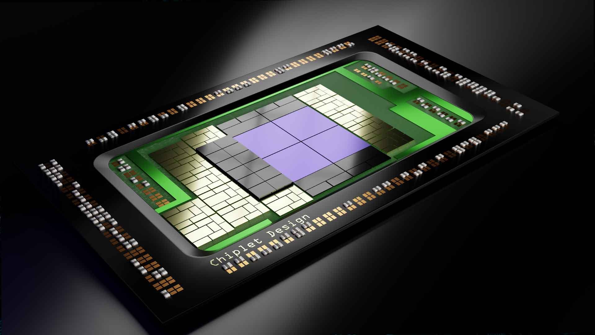
The rise of the chiplet
A chiplet is an integrated circuit with a well-defined subset of functionality, designed to be combined with other chiplets on an interposer in a single package. A set of chiplets can be implemented in a mix-and-match "LEGO-like" assembly and there are applications for microprocessors, SoCs, GPUs, and programmable logic devices across multiple use cases and markets in chiplets. Strong growth is expected throughout the 2020s.
Chiplets are the intersection between IP and the chipset business. While there are challenges, such as the fragmentation of interfaces, these are far outweighed by the benefits. Chiplets:
- are reusable intellectual property (IP) – the same chiplet can be used in many different devices.
- are a heterogeneous integration: chiplets can be fabricated with different processes, materials, and nodes, with each optimised for its function.
- lower the cost of design.
- improve the yield of the final device as chiplets can be tested before assembly to establish which dies are good.
- create business opportunities for silicon companies focusing on a specific function, especially start-ups.
I believe that some of these monolithic semis are going to use chiplets as a way of distributing some of their internal IPs in a more accessible way. So, while Intel will not turn X86 into IP, like Arm or RISC-V, it might make it available on its chiplet platform for somebody who wants to take it and combine it into their chip-based solution.
For anyone who doesn’t know Imagination, we are interested in chiplets and heterogenous systems for compute because we have a business across several IP types, namely CPU, GPU, and AI.
As such, we are an important stakeholder in the semiconductor market, and keen to help support and grow the sector. To that end, we recently published a UK-focused report on what we think should be key parts of future government policy.
Of course, like the rest of the industry, semiconductor players in the UK have a better chance of thriving if the world tackles the deep underlying structural issues and the key macroeconomic challenges we’re now facing, such as trade intensity or energy security. But I worry that as governments create policy agendas focused on local supply chains, we will lose a globally competitive, interconnected industry with nimble innovation-focused countries, such as the UK, pursuing advantage in future-facing technologies, while also working collaboratively with international partners to boost supply-chain resilience.
This approach matches well with the UK’s strengths in chip/system design and compound semiconductors, as well as general R&D and innovation. We see three strategically coherent policy levers that are available to the Government to foster the sector here.
- Supporting semiconductor research, development and design in the UK.
- Protecting and promoting UK semiconductor IP in the global value chain.
- Championing diversification through an open and outward-looking trade policy.
Despite a shift to vertical integration for the very biggest players, IP remains the best way for chip companies to develop competitive chips efficiently. Ready-made, off-the-shelf IP, also plays well with fast-follower strategies, enabling quick movers to take advantage of emerging opportunities in the market, while architecture and patent licenses can help more sophisticated customers to bring their know-how to third-party IP and IP rights and couple them more closely to increase their competitive edge.
Ultimately, third-party IP reduces costs and risks, gets to market faster and unhindered by patent trolls; enhances competitiveness, and increases time in the market, increasing revenues and profits. The IP can also be reused across multiple chip designs and different chip product lines, multiplying the benefits. All of this serves to offer a much lower total cost of ownership than trying to design complex IP in-house. Developing a chip gets you into the game; using IP helps you to win it.