Description and Features
The DDR PHY IP supports DDR5/ DDR4/ LPDDR5, provides low latency, and enables up to 5400MT/s throughput. PHY functionality is verified in NC-Verilog simulation software using test bench written in Verilog HDL. The Combo PHY IP is also able to run on DDR4, DDR5, LPDDR5 modes separately.
Features
-
Supported DRAM type: DDR5/DDR4/LPDDR5
-
Maximum controller clock frequency of 675MHz resulting in maximum DRAM data rate of 5400MT/s for DDR5
-
Maximum controller clock frequency of 400MHz resulting in maximum DRAM data rate of 3200MT/s for DDR4
-
Maximum controller clock frequency of 600MHz resulting in maximum DRAM data rate of 4800MT/s for LPDDR5
-
Interface: POD11/POD12/LVSTL05
-
Data path width scales in 8-bit increment
-
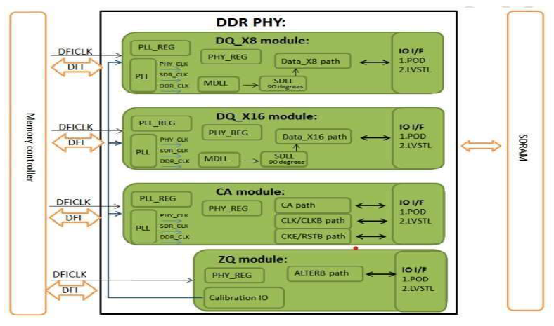
Four modules for flexible configuration:
-
CA/DQ_X16/DQ_X8/ZQ
-
Programmable output impedance (DS)
-
Programmable on-die termination (ODT)
-
Core power:0.8V, Post-driver power (VDDQ):1.1V/1.2V/0.5V, Pre-driver power(VDDP): 1.1V/1.2V/1.05V
-
Receiver power (VDDI): 1.1V/1.2V/1.05V for DDR5/DDR4/LPDDR5
-
ESD: 2KV/HBM, 200V/MM, 500V/CDM
-
Support ZQ calibration
-
Support 4 ranks by each CA module
-
Support write-leveling, CBT
-
Support PHY internal VREFDQ auto decision
-
Per-bit deskew in read and write datapath
Deliverables
-
User Manual
-
Behaviour model, and protected RTL codes
-
Protected Post layout netlist
-
Synopsys library (LIB)
-
Frame view (LEF)
-
Metal GDS (GDSII)
-
Test patterns and Test Documentation
