概述和功能介绍
The MIPI D-PHY Analog TX IP Core is fully compliant to the D-PHY specification version 1.2. It supports the MIPI Camera Serial Interface (CSI-2) and Display Serial Interface (DSI protocols). It is a TX PHY with one clock lane and 4 data lanes. The D-PHY consists of an analog front end to generate and receive the electrical level signals, and a digital back end to control the I/O functions. Internal termination resistor with auto-calibration.D- PHY is a MIPI DSI PHY (MIPI TX DPHY) Includes a PLL, a Clock Lane and four Data Lane for MIPI DSI data transmission, also D-PHY can be used as a 5V tolerance GPIO bank.
功能描述
-
Compliant to MIPI Alliance Standard for
-
D-PHY specification Version 1.2
-
Supports standard PPI interface compliant to MIPI Specification
-
Supports synchronous transfer at high speed mode with a bit rate of 80-2500 Mb/s
-
Supports asynchronous transfer at low power mode with a bit rate of 10 Mb/s
-
Supports ultra-low power mode, high speed mode and escape mode
-
Supports one clock lane and up to four data lanes
-
Data lanes support transfer of data in high speed mode
-
Supports error detection mechanism for sequence errors and contentions
-
Supports contention detection
-
Configurable skew option for each Clock and Data lanes
-
Testability for TX, RX and PLL
Deliverables
-
GDSII & layer map
-
Place-Route views (.LEF)
-
Liberty library (.lib)
-
Verilog behavior model
-
Netlist & SDF timing
-
Layout guidelines, application notes
-
LVS/DRC verification reports
Benefits
-
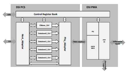
DSI PCS :
-
The Register Bank is accessible through a standard AMBA-APB slave interface, providing access to the DSI PHY registers for configuration and control.
-
Host_adapter: remappig PPI Signal with lane control and phy_adapter block;
-
Lane_ctrl block (clklane_ctrl/datalane0_ctrl/datalane1_ctrl/datalane2_ctrl/datalane3_ctrl)
-
acknowledges the operation on PPI interface. It enables a high-speed transmission or low-power transmission/reception and schedules the activities inside the link.
-
PHY_adapter: remappig lane_ctrl Signal with phy interface;
-
DSI PMA:
-
A PLL for high speed clock and MIPI data clock generation
-
Data MUX and Reference resistor calibration
-
MIPI PHY IO with GPIO compatible
Applications
-
Automotive
-
Mobile
-
IoT
-
Consumer Electronics
-
VR
-
AR
