ggNMOS intro:
For decades, a traditional workhorse device for ESD protection for standard applications in CMOS technology has been the grounded-gate NMOS device (ggNMOS).
Nevertheless, we have been explaining the operation of this device countless times, including as recently as 3 weeks ago. So, it is time for a short blog article. The schematic of a ggNMOS and its typical ESD I-V characteristic are sketched in Figure 1.a and b.
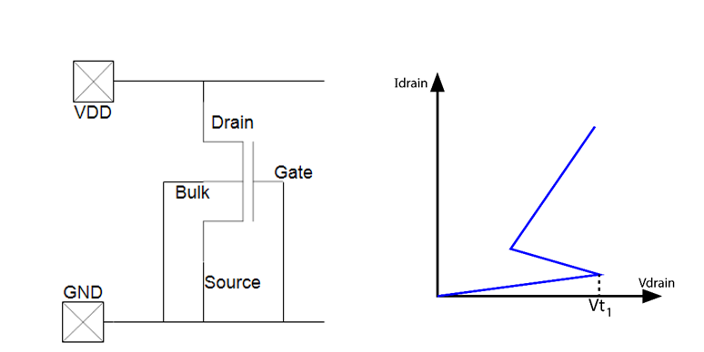
(a) (b)
Figure 1: Figure 1: ggNMOS schematic (a), and the ggNMOS IV characteristic (b).
How does NMOS snapback work?
To understand the physical operation, one should study the silicon cross-section of the NMOS (simplified in Figure 2.a), and consider the equivalent bipolar schematic that one can uncover (Figure 2.b).
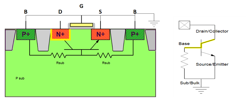
(a) (b)
Figure 2: NMOS cross-section (a) and the equivalent bipolar schematic (b).
When increasing the drain/collector voltage versus the grounded source/emitter/bulk a reverse voltage will build up across the drain to the substrate junction in Figure 2.a, which is also the collector/base diode in Figure 2.b. Until that diode breaks down (assuming no punch-through occurs) there will be no current flowing through the reverse diode or junction. At some point, the reverse diode will breakdown and current will flow in the depletion region of the diode. Carriers will be accelerated in the electric field and create an avalanche effect when knocking into other fixed carriers. This is illustrated in Figures 3 a and b. As the reverse voltage is increasing, the current will increase rapidly.
At some point, the reverse diode will breakdown and current will flow in the depletion region of the diode. Carriers will be accelerated in the electric field and create an avalanche effect when knocking into other fixed carriers. This is illustrated in Figures 3 a and b. As the reverse voltage is increasing, the current will increase rapidly.
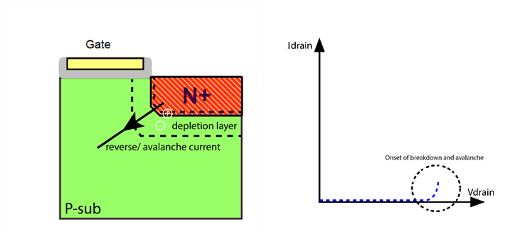
(a) (b)
Figure 3: cross-section detail: reverse junction & avalanche (a), I-V detail: breakdown & avalanche current (b).
This breakdown/avalanche current flows to ground, through the base/bulk resistor – this is the p-substrate (or p-well) resistance. We can model this avalanche current as a current source that will supply ever higher current as the voltage at the drain/collector is increased. This current source is introduced in Figure 4 a and b.
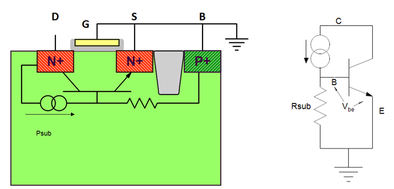
(a) (b)
Figure 4: Avalanche current source in the cross-section (a), in the equivalent schematic (b).
It shall be obvious that this avalanche current flows to the ground through the substrate resistance. A voltage will build up in the device resulting in an emitter-base bias. As soon as that voltage forward biases the emitter-base junction, the base current will start flowing. Per bipolar theory, the base current will cause collector-emitter current to flow, beta times the base current.
In NMOS structures these betas are typically large enough to sink a lot of current through the bipolar transistor. The collector-emitter voltage will drop – this causes the typical snapback in the I-V curve. This is illustrated in Figure 5.
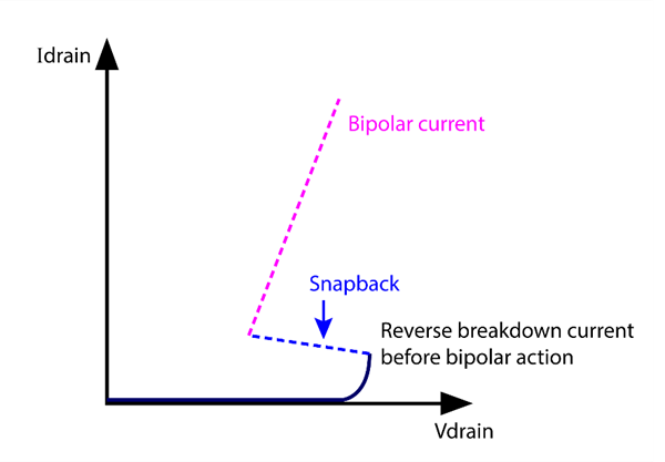
Figure 5: I-V curve of a ggNMOS.
The (ESD) current carrying capability of the parasitic bipolar in the NMOS is high as the power dissipation is somewhat deeper in the substrate, as compared to the surface channel of the device in normal MOS operation.
It is worth mentioning that we already explained in the article with the title “Time to say farewell to the snapback ggNMOS for ESD protection” why the ggNMOS is not used in advanced technology nodes such as FinFET.
