To prevent failures during production, assembly and test, IC designers include on-chip Electrostatic Discharge (ESD) protection structures at the interfaces of their Integrated Circuits. Due to continuous scaling of the processing technology, ESD remains an important reliability issue in the semiconductor industry. This article discusses TLP, the main measurement technique used by ESD experts to characterize ESD protection structures as well as the intrinsic process technology robustness or weakness.
Introduction
For decades IC engineers have used standardized models to verify the ESD robustness of integrated circuits. Each of the models represent or emulate a specific ESD stress case like ESD caused by human interaction, machine interaction or ESD stress when the chips themselves are charged.

The problem with test models like HBM (Human Body model), Machine Model (MM) and CDM (Charged Device Model) is that they only provide so-called pass/fail results. Either the device survives the required 2000V HBM, 200V MM or 250V CDM or it does not. It is hard to learn about the root cause or to study the behavior of the ESD protection devices.
In 1985, Tim Maloney from Intel proposed to use a system where ESD devices are stressed with rectangular pulses. The Transmission Line Pulse (TLP) system was already used about 40 years earlier, to characterize semiconductor devices and circuits. After the publication from Tim Maloney, several research labs created their own R&D version. The tool quickly became indispensable for the study and development of ESD protection solutions.
The first commercial TLP system was introduced by Barth Electronics through a cooperation with Koen Verhaege (while he was at Sarnoff Corporation, currently CEO at Sofics) in 1997. Several other vendors followed suit. Most of the ESD qualification facilities nowadays also offer TLP analysis.
Over the years several TLP variants have been developed, each with focus on ways to improve on the basic approach (longer and shorter pulses, higher currents, faster or slower rise time, easier connection to a wafer probe, more accurate measurement of transients, ability to measure deep-snapback, multi-level TLP, …).
TLP system construction
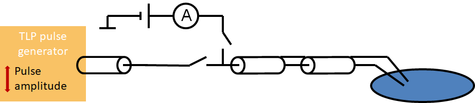
A TLP system is a kind of pulse generator. IC researchers could not rely on standard pulse generators because they needed high current levels to simulate the ESD stress. Therefore, in a typical TLP system the pulses are generated from the discharge of a charged coaxial cable of a certain length (e.g. 10m). The cable is charged up (slowly) using a high voltage DC supply at a specific voltage level
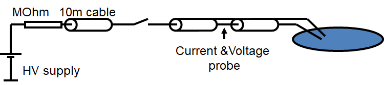
The cable is then discharged through the device under test (DUT). A fast switch or relay is used between the cable and the device. This generates rectangular pulses (pulse width of about 100ns), ideal for quick analysis on a scope.
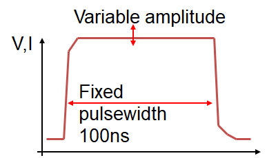
The voltage and current transients are captured on a high bandwidth (sampling) scope. The pre-charge voltage of the cable can be adjusted to generate pulses with variable amplitude.
TLP test approach
A simplified diagram shows a pulse generator (left) and a coaxial cable to connect to the device under test (DUT) depicted by a wafer. The current and voltage probes are connected to a sampling scope to record the transient pulses.
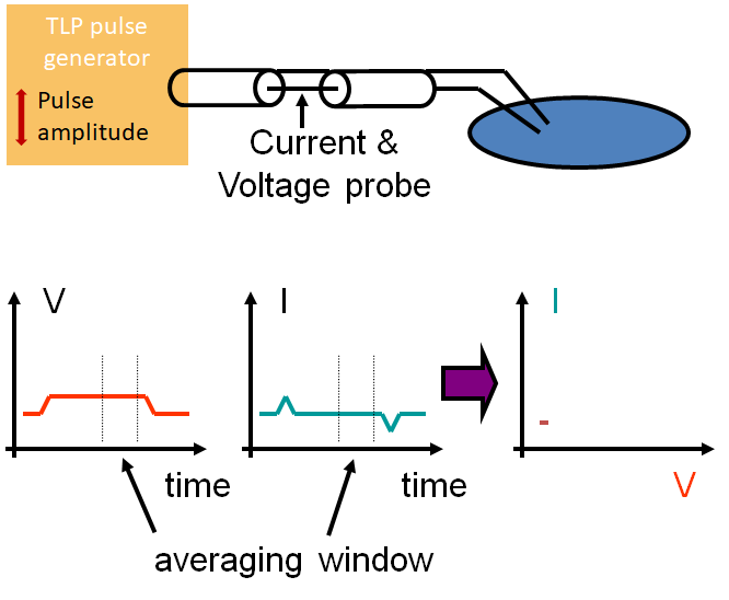
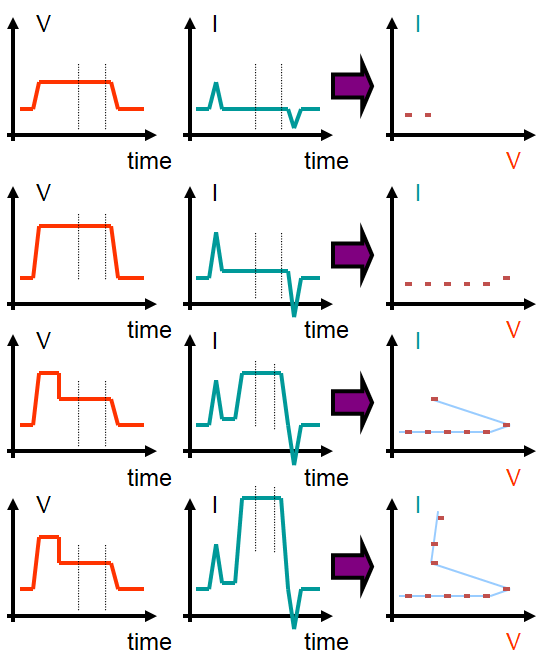
At the end of the transient pulses an averaging window is defined. E.g. for a 100ns pulse width the averaging window is between 70ns and 90ns from the start of the pulse. The voltage and current waveforms are averaged in this time window to yield a single coordinate (V, I) that is plotted on the TLP I-V characteristic.
Similar to HBM testing, the voltage level is then increased (higher voltage on the cable) and the main switch is closed again, stressing the device under test at a higher level. A next (V,I) coordinate is added to the IV-curve. This allows to build up a quasistatic IV-curve for the device and clearly shows different regions of the device behavior (off, trigger, snapback, conducting).
Failure detection
Initially researchers would look at the resulting IV characteristic to identify failure of the device. Sometimes the failure of a NMOS device would be obvious from a so-called secondary snapback. However, quickly an integrated leakage measurement was added to the TLP testers. A Source-Measure-Unit (SMU) applies a voltage bias while measuring the leakage current between the 2 device terminals.
A first leakage measurement is performed as a benchmark before the test. Then, a new leakage measurement is done after every stress pulse. This is used to create an additional curve of the leakage versus the stress current.
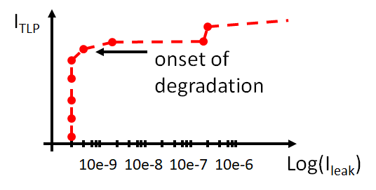
While developing the first commercial TLP system in 1996/1997, Koen Verhaege and Jon Barth realized it would be beneficial to plot both curves together in one plot. The TLP IV-curve is plotted with voltage as the bottom axis, stress current as the vertical axis. The leakage current (top axis, logarithmic scale) versus stress current (vertical) is added. This makes it super easy to spot the failure point and immediately read the corresponding failure current and failure voltage.
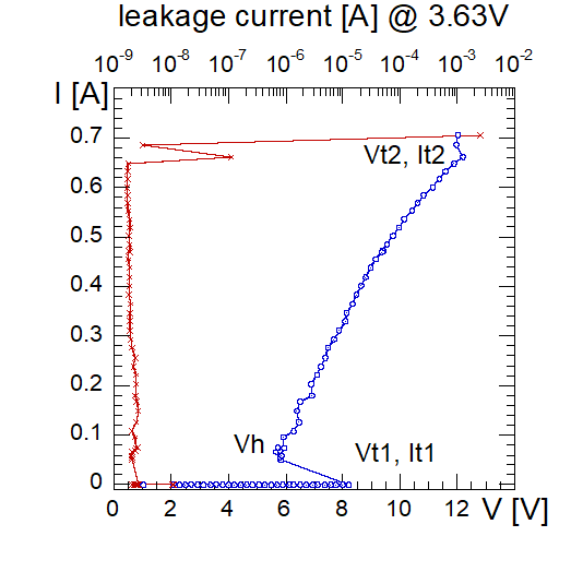
From the TLP I-V characteristic we can get information about snapback (triggering & clamping) behavior as well as maximum or failure current.
TLP at Sofics
Sofics is a foundry independent IP provider. We develop ESD protection solutions used by more than 100 fabless companies worldwide. We have validated our technology across 11 foundries, on more than 50 processes.
At Sofics we use different TLP systems. There are 2 TLP systems from Barth Electronic, a VF-TLP from the same company and additional TLP systems built using off-the-shelve pulse generators that allow to investigate ESD devices using pulses with longer duration.
Sofics engineers use TLP analysis for different reasons.
- The TLP is used to characterize the intrinsic robustness of different elements in the process (transistors, resistors, diodes) to determine the ESD design window (link). It is important to know the failure voltage of devices that should not conduct during ESD stress.
- The TLP tool is also used to learn about the maximum ESD current through the metal layers of a chip.
- Obviously, TLP is used to capture the IV curve of ESD protection devices developed at Sofics
- We also use it to characterize the ESD capability of products that our customers made
- The IV curves can also be used in ESD simulation software like the Magwel ESDi EDA tool (link).
In this way we ensure our designs are silicon proven thereby providing peace of mind for IC designers that integrate Sofics solutions into their chips.
Conclusion
The TLP approach rapidly became the main measurement tool for the ESD designer. The TLP tool allows to study ESD devices in the ESD relevant current and time domain. It really is a versatile tool for characterization of process, ESD solutions, products….
Next articles…
Follow Sofics on LinkedIn, Facebook or Twitter to stay up-to-date about our next articles, tutorials and videos. Or subscribe by email below.


3 thoughts on “Transmission Line Pulse (TLP) test system”
Comments are closed.