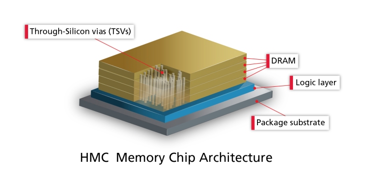
There are several reasons to combine various chiplets in a single package, either next to each other (2.5D) or stacked on top of each other (3D) like the memory cube depicted below.
For instance, it enables chip designers to select the most optimal process for each type of function (interface, memory, compute, FPGA, analog circuits, MEMS, optical, …). It also allows to create chips with larger gate count when the reticle size is the limiting factor. And of course, yield improves a lot when the area of the die is reduced.
At Sofics we get a lot of questions about the required ESD robustness for the die-2-die (D2D) interfaces between chiplets in a package. People wonder how to select the right ESD standard (HBM, MM, CDM, TLP – more info) and what robustness level (1kV HBM?) they need to design for. Furthermore people wonder how they can validate the robustness once ESD devices are integrated?
What is the right ESD standard and ESD robustness level?
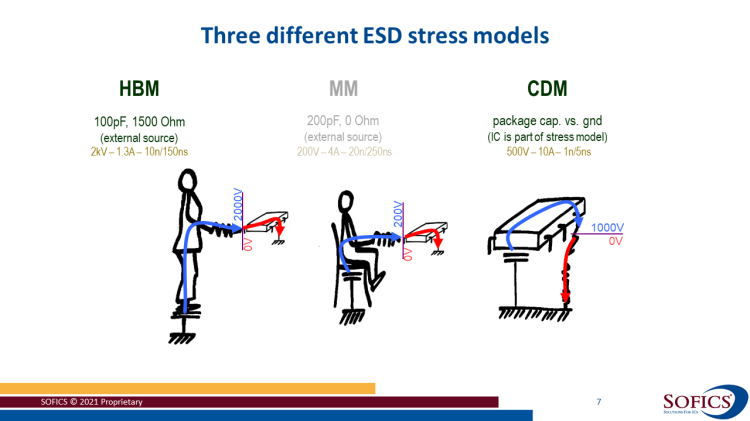
For I/O pads that connect outside the package nothing really changes. The typical HBM, MM and CDM requirements are still valid. During assembly of the chip packages on the PCB board, ESD events can occur. IC pins can touch humans, machines or surfaces on another potential, leading to a discharge,
For clarity: For years there is an industry initiative to reduce the robustness levels (e.g. from 2kV HBM to 1kV HBM). The group argues that semiconductor chip and PCB assembly these days occurs at much tighter ESD controlled facilities, reducing the number and severity of the ESD events. Another great reason to reduce the levels is that it enables higher bandwidth and finally it can also reduce total ESD area. On the other hand there is another, opposite trend to actually increase the robustness (to 8kV HBM or even 8kV IEC 61000-4-2. more info) for certain types of interfaces (HDMI, USB, …) or applications (automotive).
However, (D2D) interfaces that stay inside the package are clearly different. Once integrated in the package it is not possible to touch the I/O pads. So, it is logic that the HBM/MM/CDM standards do not apply anymore. But is it possible to leave out dedicated ESD protection completely for those pads? Probably not.
ESD events relevant for chiplets
An HBM or MM event applied between two pins of an integrated circuit (IC) can impact the die-2-die interfaces. Suppose the pin stressed (e.g. 2kV HBM) connects to one chiplet and the grounded pin connects to another, adjacent chiplet. Clearly the charges need to travel between those chiplets to close the loop. Similarly, for CDM, the IC can get charged up for instance by gliding down a tube. Charges are distributed across the entire IC, on the package leads, on the package, the interposer, and across every chiplet. All these charges need to find a discharge path to the single grounded pin. During the CDM event, charges will travel from one chiplet to the next before reaching the grounded pin.
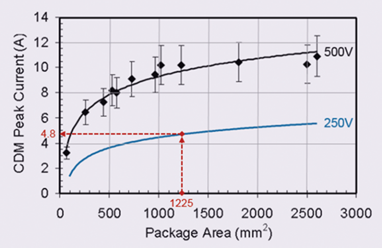
Once the chiplets are integrated on the package substrate, currents during ESD events like CDM will be distributed across many die-2-die connections. This means that the ESD protection cells for an individual interface can probably be reduced in robustness level and size. The amount of (total) CDM current still depends on the size of the entire package, shown below. Typically co-packaged dies for AI or communication applications are in rather large size packages, so the total CDM current will be high.
The amount of sharing of the ESD current between interfaces depends on the selected clamps, the resistance and location of the interfaces and the power grid. The amount of CDM current from one chiplet to the next also depends on their size and charge distribution.
However, there still could be ESD events during the assembly of chiplets where charge is not distributed. When the chiplet is charged differently than the substrate there will be a spark (like CDM) when they approach each other. Probably a single bump (which is closest) will see most or all of the current. For sure, assembly houses will try to keep all elements at roughly the same potential. However, for designs in advanced nodes with sensitive thin oxide interfaces, even a small voltage difference can cause a failure. If the assembly process is tightly controlled, then the potential difference between the two elements will be almost zero. The assembly partner should have some information about that aspect.
In the end this means that the people responsible for the assembly of the chiplets must be able to give a guideline in whatever standard or form. That are the guidelines we have used for our customers when they asked us to design for e.g. 100V HBM (examples). It is possible, maybe even likely, those are an overkill.
People in the industry are confused about the right ESD protection standard to follow AND which level to design for. It seems designers are also proposing to further reduce the robustness in order to reduce area (external link)
That is an expectation and mostly a wish from the IC designers to reduce the total (ESD) area. It is probably not based on reliability data of actual products. Moreover, it remains difficult to translate the 10V or 5V CDM level to an amount of current (peak current of ~10mA?) because the size of the chiplet influences that. That amount of current is needed to calculate/estimate the size of the junctions for the ESD devices
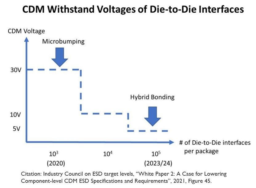
🆕🆕🆕NEW: August 2023: The industry council on ESD targets has released a new document (link) targetting die-2-die interfaces. They ran a survey and have looked at different aspects (process control, testing, pre-silicon verification and simulations).
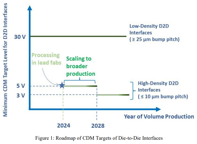
The conclusion is that they are lowering the current 30V CDM target level to 5V and later 3V for extremely dense interfaces. The drop to 5V is possible already in 2024 for some leading assembly fabs (with strong ESD control).
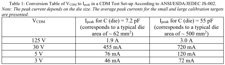
They also offer a translation of these voltage numbers to an amount of peak current that can be used to design the ESD clamps. 🆕🆕🆕.
Some people even say that they would not add any ESD devices for Tx circuits (there are parasitic diodes integrated) and minimal protection for Rx (gate) only.
Feel free to contact Sofics to discuss your own chiplet design. No matter what ESD standard and robustness level is selected, specialty I/O and ESD protection is required.
Some links for further reading;
- 🆕 August 2023: White paper on ESD protection for die-2-die interfaces: link
- White Paper 2 on CDM – https://www.esdindustrycouncil.org/ic/en/documents/white-paper-2-a-case-for-lowering-component-level-cdm-esd-sp
- Bunch of Wires: BoW – https://opencomputeproject.github.io/ODSA-BoW/bow_specification.html#sec-scope
- UCIe homepage: https://www.uciexpress.org/ and general intro: https://www.uciexpress.org/post/how-ucie-will-enable-broad-chiplet-adoption
- ESD protection for 2.5D and 3D packages: https://monthly-pulse.com/2021/02/12/esd-protection-for-2-5d-and-3d-packages/
- Article about the different approaches and ecosystems: https://semiengineering.com/mini-consortia-forming-around-chiplets/