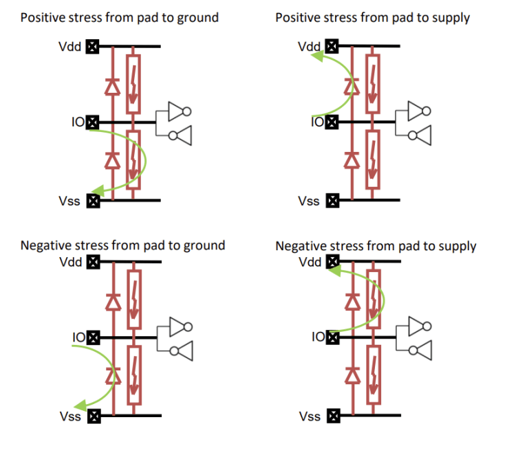
ESD protection in the most advanced FinFET technology is challenging: The ESD design window (link) is extremely narrow in FinFET processes (link). Moreover, some of the conventional ESD solutions like the ggNMOS based protection are not effective anymore (link).
To protect sensitive FinFET circuits IC designers need to design the traditional ESD clamps and diodes a lot bigger. It is also required to reduce the distance between rail clamps and interface pads. It leads to an increase in ESD related area and increase in parasitic capacitance at the interfaces from scaling up the ESD (dual) diodes.
Fortunately, Sofics’ proprietary on-chip ESD protection clamps are proven to protect sensitive FinFET circuits against ESD events without requiring such a huge increase in area. Even better, the measurements from our recent test chip on TSMC 3nm show great potential for area reduction.
TSMC-Sofics partnership
This year (2023), the TSMC Open Innovation Platform® (OIP) turns 15. Already at the start in 2008, Sofics joined the TSMC Design Center Alliance (DCA). Two years later we also joined the IP alliance (link).
TSMC’s OIP goal has been clear from the start: shortening design time, time-to-market and time-to-revenue. 15 years ago, TSMC started building what became the largest ecosystem of IP (intellectual property) blocks, silicon-proven on their foundry processes. They gathered IP blocks from IP providers like Agile Analog, Analog Bits, Andes Technology, ARM, Etopus, M31, Mixel, Silicon Creations,..,

To ensure the quality of the IP blocks, providers like Sofics need to follow the TSMC-9000 assessments (link). It involves uploading design information before the tape out, at tape out and after characterization.
Sofics engineers have validated our proprietary ESD clamp solutions on almost every TSMC process technology (BCD, CMOS, FinFET). These silicon-proven IP blocks are integrated in designs from 60+ TSMC customers in a broad set of applications spanning AI, automotive electronics, datacenter wired & optical communication, medical systems and various wireless interfaces (link).
Sofics’ IP available on TSMC 3nm
Over the last 5+ years, Sofics has validated its IP on the earlier FinFET processes including 16nm, 12nm, 7nm, 6nm and 5nm technology at TSMC. In January 2023 we taped out our test chip on a 3nm MPW run.
On the 3nm test chip we validated a whole range of ESD clamp solutions
- Power or rail clamps for 0.75V, 1.2V, 1.5V, 1.8V, 2.5V and even 3.3V
- Full local protection concepts for interfaces on different voltages
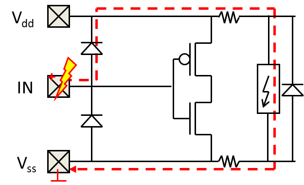
Sofics has applied a local clamp concept for many years to protect the most sensitive interface circuits. You can read more about it in several articles (link, link, link, link). The use of proprietary Silicon Controlled Rectifier (SCR) devices strongly reduced required area, leakage current and parasitic capacitance compared to conventional approaches.
Below is an example of an on-chip ESD protection clamp for 3.3V interfaces/domains measured on the 3nm test chip. The reference clamp on the test chip can achieve 2kV HBM and can easily be changed to other robustness requirements. The clamping (or holding) voltage is well above 3.3V (+10%) to ensure high latch-up immunity. The trigger voltage can be adapted to align to the design window of the functional circuit that needs protection.

Sofics’ rail clamp validated on TSMC 3nm
Recently we developed a new rail ESD clamp approach that can be integrated into Vdd/Vss pads. The novel technique can be applied to different voltage domains and has the potential for strong area savings.
On the 3nm test chip we compared Sofics’ new solution with the traditional rail clamp solution (BIGFET or active MOS with RC-based trigger) used by many designers in the industry. Sofics’ proprietary clamp achieves a 66% area reduction compared to the industry reference approach (press release).
The reference design of the 0.75V rail clamp on our test chip achieved 10 A TLP (100ns) and more than 8kV HBM. It also reached more than 15A on the VF-TLP tester, perfect for protection against fast transients like CDM.

Of course many applications do not need such high ESD protection levels. The clamp design can be scaled down to more typical ESD levels easily. This further reduces the silicon footprint to less than 700 um² for 4kV HBM and less than 450 um² for 2kV HBM. This small area enables a lot of flexibility to integrate the rail clamp in small I/O segments used in BGA devices. It can also be integrated together with the ESD diodes for sensitive I/O circuits that are further away from a Vdd pad.
Conclusion
Thanks to the partnership with TSMC we could validate our proprietary ESD clamps on the most advanced FinFET process (3nm) that is available for production today (2023).
Sofics technology provides benefits like higher IC performance and higher robustness. IC designers preparing a product can also reduce design and manufacturing costs. The newest innovation enables a great area saving potential. For the 3nm node a 66% area reduction is demonstrated for the 0.75V rail clamp.
Contact us (info@sofics.com) to discuss your IC design constraints or if you’d like to schedule a video call about our 3nm FinFET solutions.
Next articles…
Follow Sofics on LinkedIn to stay up-to-date about our next articles, tutorials and videos. Or subscribe by email below.