
1. Introduction
Choosing the right type of memory is critical to ensure that the power and performance requirements are met for the target application. Memory technologies have significantly evolved over the last years, providing tailored solutions for a variety of applications such as Graphics cards, game consoles, high-performance computing, and artificial intelligence (AI) all have specific requirements regarding throughput, speed, and latency.
One type of memory that stands out is GDDR memory, which provides exceptional bandwidth, low latency at a reasonable cost. The new GDDR7 memory is suitable not only for graphics applications but also well-suited for Edge AI, Robotics, compute, industrial, autonomous driving, and other applications requiring high bandwidth memory solutions. These applications can highly benefit from this new memory type.
This white paper will discuss the design challenges that IC designers are facing when developing the new GDDR 7 high-performance memory interface and highlight some of the possible solutions to overcome these challenges, ensuring compliance and robustness of the GDDR7 memory interface.
2. The Evolution of the Graphics DDR Memory
The first GDDR (Graphics Double Data Rate) memory was introduced by Samsung Electronics in 1998. It was initially known as DDR SGRAM (Double Data Rate Synchronous Graphics RAM) and was designed to meet the high-bandwidth requirement of a graphics processing unit (GPU). This innovation of a graphic-workload-specific memory type was initially driven by the rapid rise of the gaming console market, which required higher frame rates and high resolutions. Throughout the evolution of this specific type of memory, each new version has improved bandwidth performance, speed (frequency), and power consumption.
The use of graphics cards and GPUs, specifically by NVIDIA, for non-graphic applications such as scientific and AI applications, has further accelerated the innovation of GDDR memory, leading to several new features to break the memory speed limits. For example, GDDR6X utilizes PAM-4 (Pulse Amplitude Modulation 4-level), which uses four distinct signal levels, allowing it to transmit two bits per clock cycle and doubling the data rate of the previously used NRZ coding in GDDR6. While PAM-4 offers significant advantages in terms of data rate and bandwidth efficiency, it does come with some drawbacks. First, PAM-4 is more complex than traditional NRZ signaling, leading to increased design and manufacturing challenges. Second, PAM-4 can be less power-efficient in some scenarios, as the increased number of signal levels can lead to higher power consumption. Third, PAM-4 causes Signal Integrity Issues as the signal is more susceptible to noise and signal degradation. The closer spacing of the signal levels makes it more challenging to maintain signal integrity, especially over longer distances. Fourth, implementing PAM-4 can increase the overall cost of the memory system due to the need for more sophisticated error correction and signal processing techniques.
The new GDDR7 was developed to overcome these challenges by implementing PAM-3 and adding on-die error correction, error checking, and scrubbing to improve memory reliability, which is particularly useful for high-performance computing and AI applications.
The first generation of GDDR7 achieves data rates of 32 Gbps per pin. However, the JEDEC GDDR7 standard allows for a performance level of up to 48 Gbps per pin and memory throughput of 192 GB/s per GDDR7 memory device. This makes it especially attractive for other GPU applications such as AI accelerators and AI inferencing, as it satisfies the requirements for high memory bandwidth and demanding workloads.
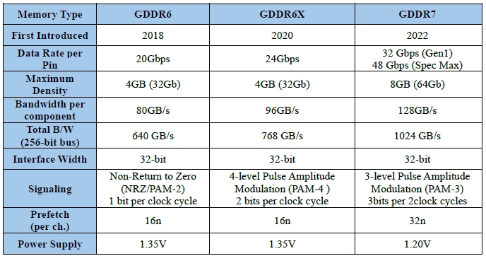
Table 1: Comparison of Different GDDR Memory Types
3. GDDR7 Key Design Challenges and Solutions
IC designers will encounter several challenges when creating a GDDR7 memory interface, which includes both a PHY and a controller.
PAM-3
GDDR7 provides dual-mode signaling and offers the flexibility to optimize for both performance and power efficiency, depending on the workload. The PAM-3 encoding mode is used for high-speed data transfer, enabling data rates up to 36 Gbps per pin. The NRZ encoding mode is used for lower speeds but is more energy-efficient.
The PAM-3 encoding in GDDR7 is quite complex and deserves a White paper on its own. Here are some of the key points which need to be considered.
- The PAM-3 Eye diagram has two eyes that need to be free of noise and distortion for reliable data transfer.
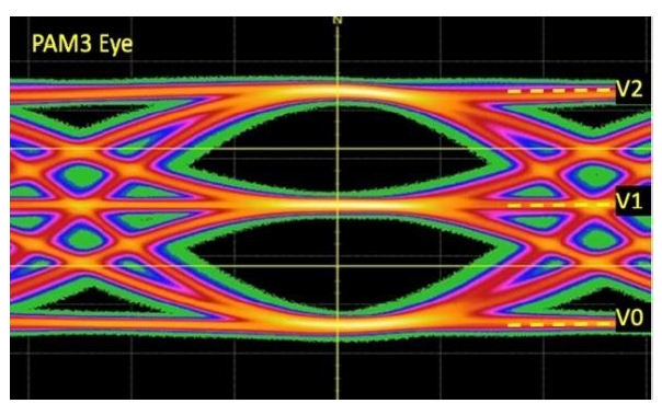
Figure 1: PAM-3 Eye Diagram
- The Data Payload encoder/decoder, which is responsible for providing the right data in the right order to the memory interface lanes (DQ[9:0], DQE ), utilizes several coding schemas to scramble the data. Consequently, the design requires intensive synchronization.
Signal Integrity
When operating at extremely high data rates, such as the GDDR7 (32 Gbps), maintaining a good electrical signal, which ensures that the transmitted data is reliable, becomes challenging. Taking a deeper look, the diminishing signal integrity can have different causes, calling for different improvement methods to be applied.
Power Integrity
Ensuring a stable and clean power delivery network (PDN) to all parts of the chip and its subsystems is important to guarantee stable and reliable operations. IC designers are advised to carefully analyze and evaluate any kind of IR drop (voltage drop due to resistance in power lines), Dynamic voltage drop (due to switching activity), Ground bounce, and Decoupling capacitor placement.
De-emphasis
De-emphasis is a signal processing technique used to improve signal integrity. When electrical signals travel through channels like printed circuit boards or cables, they can experience losses and distortions due to factors like resistance, dielectric properties, and signal reflections. De-emphasis helps counteract these issues.
During signal transmission, high-frequency signals are typically attenuated faster than low-frequency signals. De-emphasis technology compensates for this high-frequency attenuation by reducing the amplitude of low-frequency signals. This will increase the relative amplitude of high-frequency signals compared to the low-frequency signals. This method ensures a more intact high-frequency signal component at the receiver. By reducing the overall signal amplitude, de-emphasis effectively minimizes electromagnetic radiation. This is critical for reducing electromagnetic interference (EMI), particularly in environments with stringent electromagnetic compatibility (EMC) requirements.
De-emphasis uses different techniques for the receiver and transmitter. At the transmitter end, the amplitude of certain parts of the signal is reduced (or "de-emphasized") based on the signal's data pattern. This is often done to balance the frequency components of the signal. The receiver then uses equalization techniques to restore the signal to its original form, compensating for the losses and distortions introduced by the transmission channel. De-emphasis ensures reliable communication at gigabit speeds and is a critical method for maintaining performance.
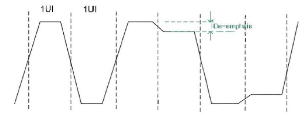
Figure 2: High-Frequency Attenuation
Mitigating Inter-Symbol Interference (ISI)
Mitigating inter-symbol interference (ISI) in chip design is crucial for ensuring reliable high-speed data transmission. ISI occurs when signals from adjacent symbols overlap, causing distortion and errors. ISI uses a large set of mathematical methods, such as equalization, pulse shaping, pre-emphasis, de-emphasis, and error correction.
Specifically, for the GDDR7 PHYs, data recovery is extremely challenging because, as data rates increase, the Unit Interval (UI) (symbol duration) becomes significantly smaller. For example, GDDR7 provides an effective data rate of 32 Gbps, which results in a UI of 62.5 ps with PAM-3 modulation. This means that for every 62.5 ps, one PAM-3 symbol is being transmitted. This shrinking UI has a significant impact on the preceding bits and all subsequent ones, making it difficult to detect the correct data. If unaddressed, such interference can cause the Bit Error Rate (BER) to surge. A critical scenario occurs when consecutive 1s (or 0s) are followed by a 0 (or 1). In such cases, the signal voltage may fail to reach the required level due to residual effects from prior bits, as illustrated below. This phenomenon, where earlier signals distort later ones, is termed Inter-Symbol Interference (ISI).
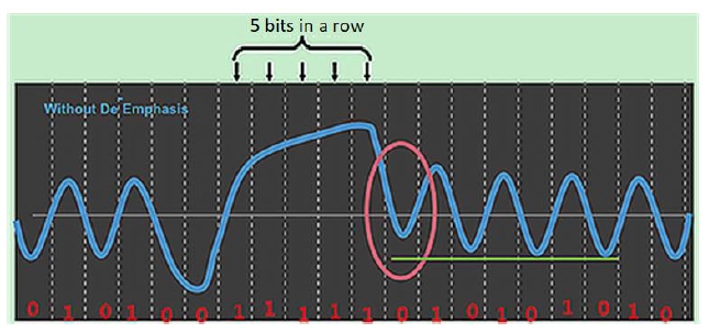
Figure 3: Mitigating Inter-Symbol Interferences (ISI)
Optimizing Eye Diagram Quality
De-emphasis is a method used to enlarge the eye opening in the eye diagram. Resulting in an improved data signal, which allows the receiver to read the data signal easily and more reliably. This helps the receiving end to accurately recover the original data and reduce the error rate.
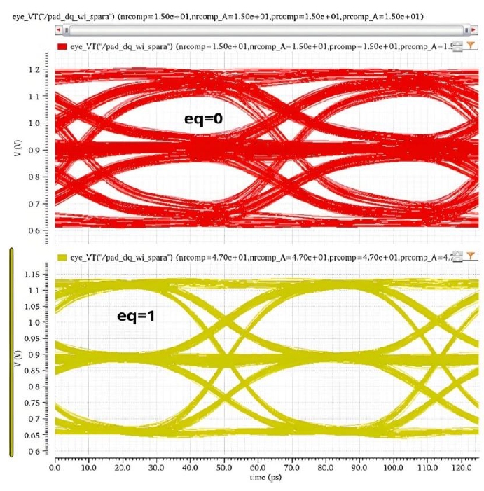
Figure 4: Optimizing Eye Diagram Quality
Considerations when using de-emphasis
While the de-emphasis method seems to address various GDDR7 design challenges, it comes with numerous drawbacks, which require careful consideration and expert knowledge.
Amplified Crosstalk: If crosstalk exists on the data transmission line, de-emphasis may amplify the high-frequency crosstalk components. Crosstalk is usually more predominant in the high-frequency spectrum of a signal, and de-emphasis will increase the relative amplitude of high-frequency signals. Therefore, it increases the crosstalk of the signal. It is recommended to consider the impact of crosstalk when using the de-emphasis method and take corresponding measures to suppress the crosstalk.
Reduced Signal Amplitude: The De-emphasis method reduces the signal amplitude to achieve compensation for high-frequency losses and distortion, which may lead to a decrease in the signal amplitude during transmission. However, in some cases, the signal amplitude is reduced too much, which may affect the signal reception quality. Therefore, it is necessary to reasonably adjust the degree of the de-emphasis method and ensure that the signal amplitude is still high enough at the receiving end.
Configurability and parameters: To cope with the complex link environment and the different parameter combinations of de-emphasis, a training mechanism needs to be implemented to obtain the optimal parameter values.
Decision Feedback Equalizer (DFE)
A Decision Feedback Equalizer (DFE) (Figure 5 DFE) is a type of adaptive equalizer used in chip design to mitigate inter-symbol interference (ISI) during high-speed data transmission. In a GDDR7 PHY, the DFE is one of the core methods used for signal integrity improvement at the receive side, especially at high data rates above 24 Gbps. The DFE restores the highfrequency signal by dynamically canceling inter-symbol interference (ISI).
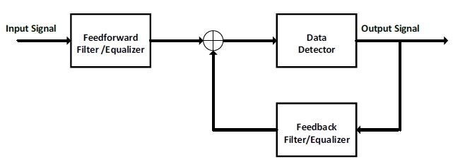
Figure 5: DFE
Signal integrity improvement is achieved by dynamically canceling inter-symbol interference (ISI). Some of the core functions that are used in a DFE are:
Feedforward Equalizer (FFE) combined with Feedback Equalizer: This function will provide preliminary compensation for high-frequency attenuation in the feedforward filter. The feedback filter calculates the amount of interference for subsequent symbols based on the history of the adjudicated symbols and reverses the offset.
Signal Filtering: FFE operates as a finite impulse response (FIR) filter. It creates delayed versions of the input signal and combines them with specific weights to counteract inter-symbol interference (ISI).
Pre-Cursor and Post-Cursor Taps: The filter uses "taps" to adjust the signal. Pre-cursor taps address interference caused by earlier symbols, while post-cursor taps handle interference from later symbols.
Multi-Tap Structure: A Multi-Tap Structure in chip design refers to a configuration used in equalizers, clock tree synthesis, or signal processing systems to enhance performance and mitigate issues like inter-symbol interference (ISI).
Equalizers: In a signal equalizer, a multi-tap structure is used to create multiple delayed versions of the input signal. These "taps" are weighted and combined to counteract distortion and interference. For example, Feedforward Equalizers (FFE) and Decision Feedback Equalizers (DFE) often use multi-tap structures.
Clock Tree Synthesis: Multi-tap structures can be applied in clock tree synthesis to distribute clock signals efficiently across a chip. This helps reduce clock skew and improve timing performance, especially in high-performance processors.
Signal Processing: Multi-tap filters, such as finite impulse response (FIR) filters, use multiple taps to shape signals and remove unwanted noise or distortion.
It is common practice to use a multi-tap structure in high-speed communication systems and advanced chip designs to ensure signal integrity and optimize performance. In the design of a GDDR7 PHY, a multi-tap DFE is used, where each tap corresponds to a different delayed symbol history. The tap coefficients are computed in real time by an adaptive algorithm (e.g., LMS algorithm) to match the channel characteristics. The algorithm follows the following mathematical expression:
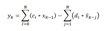
Where ci is the feedforward coefficient; dj is the feedback coefficient; 𝑥̂ is the sign after judgment.
Compared with the traditional NRZ signal coding schema, the GDDR7 memory interface uses PAM-3 coding, which increases the complexity of the DFE design further, and IC designers will meet more challenges than before.
Symbol Decision Complexity
Symbol complexity makes the design of a GDDR7 PHY more complex and challenging. While the traditional NRZ coding schema uses only NRZ, which encodes the signal into a binary value (0/1), it requires only a single-threshold decision (e.g., above mid-level = 1, below = 0). In this case, the DFE feedback path calculates interference simply, based on the binary value of the previous symbols and their impact on the current symbol.
However, PAM-3 uses a three-level signal coding (-1, 0, +1), which requires dual-threshold decisions (e.g., above +Δ = +1, below -Δ = -1, mid-range = 0). In this case, the complexity of the decision logic increases significantly, demanding multi-stage comparators and more complex decision circuits.
Inter-symbol interference may arise from multiple combinations of adjacent symbol levels, requiring more complex feedback calculations.
Noise Margin & Equalization Precision
GDDR6 NRZ coding uses larger voltage spacing (ideally 0.675V, 1.35V), providing a higher noise margin. In this case, the DFE coefficient adjustments are more tolerant of bit error rate (BER) degradation.
In GDDR7 PAM3, 3 reduced voltage spacing (ideally, 0.6V, 0.9V, 1.2V) is used, which lowers the noise margin by ~3 dB. In this case, the DFE requires higher equalization precision to avoid misjudgment due to smaller Unit Interval (UI) spacing, and a finer or more granular coefficient calibration is needed (e.g., Least Mean Square (LMS). These algorithms demand higher convergence accuracy and increase design complexity.
Complexity of Inter-Symbol Interference (ISI)
In case of NRZ coding, ISI primarily stems from single-level transitions between adjacent symbols (0→1 or 1→0), resulting in simpler interference patterns, which allows for a DFE design with only a few taps (e.g., 3–5 taps).
PAM-3 on the other side uses a three-level signaling, which introduces more complex ISI patterns (e.g., -1→0→+1, +1→0→-1, etc.). This requires the DFE design to use more taps to cover longer channel responses (e.g., 5–7 taps), and the feedback paths must handle multi-level historical data, significantly increasing computational and DFE design complexity.
An optimized DFE function will significantly improve signal performance and power consumption. A well-designed DFE can improve the opening of the eye diagram by 30% without a significant increase in area and power consumption of the IC.
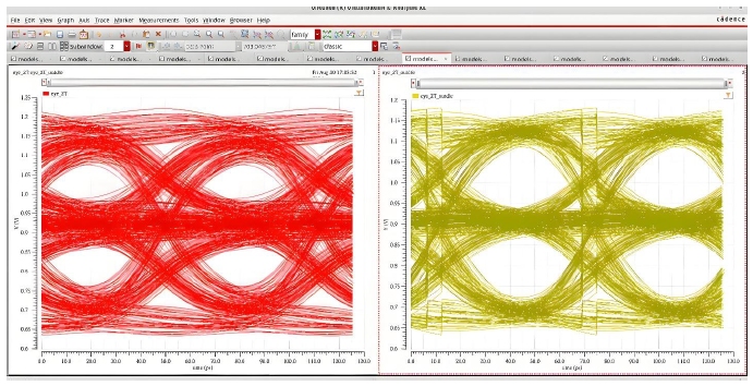
Figure 6: Eye diagram improvement with DFE
Reference Voltage (Vref) Accuracy
The GDDR7 memory interface uses a PAM-3 (3-level Pulse Amplitude Modulation) for signal encoding schema. Consequently, the receiver must properly decode the receiver’s signal. In practice, this means that the receiver compares the signal voltage against the reference voltage (Vref). The accuracy of Vref directly affects reliability and proper signal decoding. An inadequate precision of Vref may lead to misinterpretation of signal levels and will result in an increased bit error rate (BER).
Especially for high-speed signals using three-stage signals, an accurate and precise Vref is a must-have requirement to ensure robust data transmission. Higher Vref accuracy ensures better alignment with the actual signal mid-level voltage, minimizing errors caused by voltage drift or noise. As the amplitude decreases for high-speed signals due to channel loss (e.g., similar to DDR5’s PODL signaling), a precise Vref maximizes the "eye diagram" opening, improving tolerance to noise, crosstalk, and power supply fluctuations. GDDR7 operates at 32 Gbps, which results in a much shorter signal rise/fall time, reducing both horizontal eye opening (UI) and vertical amplitude. Precise Vref ensures reliable sampling within tighter voltage and timing windows.
PVT Variation Compensation
Vref is susceptible to process, voltage, and temperature (PVT) variations. High-precision Vref implementation must integrate dynamic calibration circuits (e.g., Distributed Thermal Sensor (DTS)/Dynamic Core Coupling (DCC)) to adapt in real-time to a changing environment, ensuring stability across all operating conditions. A precision power management circuit (e.g., LDOs or dedicated Vref generation modules) must be implemented to reduce the sensitivity of noise in the power supply, which minimizes the supply ripples and strengthens the system’s power immunity.
Controller Performance Optimization
The GDDR7 memory subsystem contains a couple of performance improvements, relevant to the memory controller, to overcome the challenges of proper data communication, such as the following times:
- Read data reordering to resolve protocol-level issues caused by out-of-order command execution during optimization.
- Multi-port arbitration policies to balance read/write switching and ensure high-priority commands are efficiently scheduled.
- Address conflict resolution for read/write operations to improve consistency and reduce delays from blocked SoC-level commands.
- Write command consolidation to reduce operations involving write masks and eliminate redundant commands.
- Dynamic read/write direction switching to minimize timing delays such as tWTR, tRTW, and tRCD.
- Kernel-level scheduling to prioritize urgent or high-priority commands under bandwidth pressure.
The scope of these challenges and solutions is beyond the scope of this paper, and we may discuss it in a separate white paper in the future.
4. GDDR7 Economics when Bandwidth Matters
As many types of memories exist, such as DDR, LPDDR, HBM, and GDDR (Figure 7 Memory Bandwidth per Memory Type). GDDR7 outperforms any other type of memory in terms of memory bandwidth cost (Table 2 Bandwidth / Cost Ratio). It provides the best bandwidth-to-cost ratio and should be the first choice for applications requiring a cost-optimized high bandwidth memory.
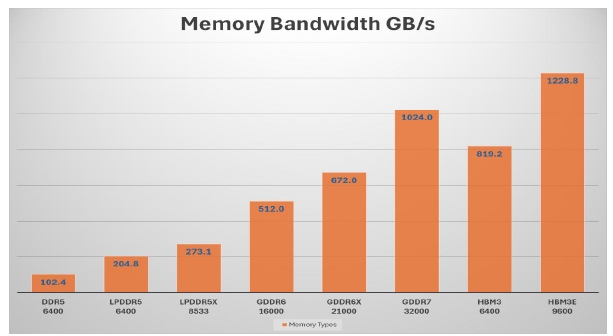
Figure 7: Memory Bandwidth per Memory Type
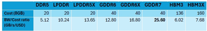
Table 2: Bandwidth / Cost Ratio
Note: The calculations in Figure 7 Memory Bandwidth per Memory Type) use the following bus width DDR5- 16 Byte, LPDDR5/5X - 32 Byte, HBM3 and HBM3e – 128 Byte.
5. Silicon-Proven GDDR7 Interface IP
Innosilicon has an extensive high-speed memory interface IP portfolio, including GDDR7/6X/6, HBM4/3E, LPDDR6/5X/5, and MRDIMM DDR5, DDR5, UCIe Chiplet, and others.
In 2018, Innosilicon became the world's first GDDR6 IP provider and was publicly recognized by Micron as an innovation leader. The company offers a silicon-proven GDDR6/6X IP, reaching up to 24Gbps, and building on that knowledge, developed a cutting-edge GDDR7 IP solution, which includes PHY, controller, and verification environment with industry-leading PPA (Power, Performance, and Area) optimization. The IP supports all JEDEC-compliant GDDR6, GDDR6X, and GDDR7 components available on the market.
Innosilicon 's flexible GDDR memory portfolio is easily customizable and available for all leading foundries and process technologies. All IP are available with signal integrity and power integrity analysis, verification models, prototype, and simulation support. Innosilicon's GDDR6/6X/7 solutions have been highly recognized by many AI manufacturers worldwide and are one of the leading “easy-to-integrate” IPs in the market. The GDDR6/6X IP is silicon-proven with a very mature production basis, which is unique in the world. Innosilicon’s experience in GDDR6/6X has helped to develop the new GDDR7 IP, achieving data rates of 32 Gbps and even 40 Gbps.
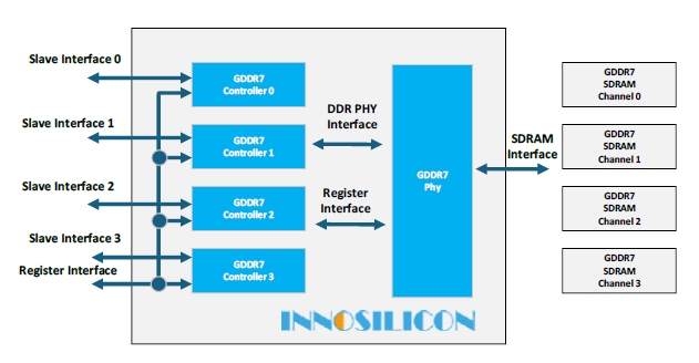
Figure 8: Innosilicon GDDR7 Subsystem (Controller & PHY) Solution
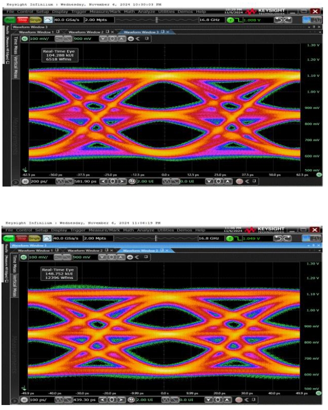
Figure 9: GDDR7 Eye Diagram 32 Gbps (top), 40 Gbps (bottom)
Innosilicon’s GDDR7 IP is silicon-proven, highly customizable, and ready for integration. It supports multiple process technologies & foundries from 8nm to 3nm.
Feature Highlights:
- GDDR7 with data rates up to 32Gbps in volume production
- Adaptive De-emphasis algorithm for compensation of insertion loss and improved signal integrity
- CTLE (Continuous Time Linear Equalization) at the receiver for improved signal integrity and ISI compensation
- DFE (Decision Feedback Equalizer) for compensation of ISI and improved signal integrity
- High precision reference Voltage, with step sizes less than 2.4 mV, for best-in-class signal integrity
- Offset calibration compensating the voltage offset at the receiver, improving sampling margin
- Tcoil topology for increased bandwidth
- Driver strength and ODT auto-calibration
- Auto Training with training pattern generator and periodic retraining function for easy compensation for PVT variations
- Inline ECC function, for improved data integrity
- AXI pseudo channel functions for faster execution of high-priority commands
- Address hash mapping for improved efficiency of random data access
- Data Encryption function for improved data security
- On-Die ECC & On-die scope
6. Summary
GDDR memory has experienced a significant amount of innovation over time. Initially designed for video game applications, it has now expanded into areas such as Edge AI, Robotics, compute, industrial, autonomous driving, and other applications requiring high bandwidth memory solutions. GDDR7 memory offers an outstanding blend of high performance, high bandwidth, and low latency, making it highly advantageous in terms of both performance and power consumption.
Designing a robust and reliable GDDR7 memory interface is a complex undertaking. The extremely high data rate and the PAM-3 signal coding scheme are challenging system designers to implement sophisticated algorithms while limiting silicon area and reducing power consumption. Extensive knowledge and experience are necessary to optimize time-to-market and drive the SoC to volume production.
Inosilicon is the world’s leading IP provider for GDDR7 and has extensive experience in designing high-speed interface IP. The company was the world's first GDDR6 IP provider, publicly recognized by Micron, and has a proven track record of developing easy-to-integrate GDDR IP with industry-leading PPA (Power, Performance, and Area) optimization. The IP is fully JEDEC-compliant and supports all GDDR6, GDDR6X, and GDDR7 components available on the market. Innosilicon’s first-generation GDDR7 PHY IP is silicon-proven and has already achieved 32 Gbps in mass production.
7. About Innosilicon
Innosilicon is a leading global provider of High-Speed IP and ASIC design services (front-end and back-end design), enabling customers to shorten time-to-market, reduce risk, and design cost. The unique system know-how turbocharges any SoC design by providing a complete subsystem.
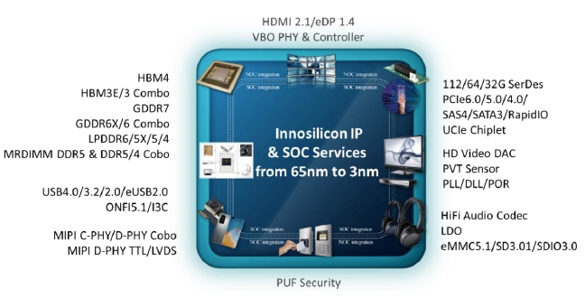
Figure 10: Innosilicon’s Subsystem Offering
Founded in 2006, the company has established itself as a reliable IP provider and is well-recognized in the semiconductor industry. Innosilicon supported over 300 top-tier clients, reducing time-to-market and limiting design risk, shipping more than 10 billion high-end SoCs and developing silicon solutions in FinFet processes across all major foundries. Innosilicon is committed to driving global innovation by leveraging its extensive chip design expertise and deep partnerships with semiconductor foundries, like TSMC, Samsung, Global Foundries and others, striving toward customer success.
Innosilicon stands at the forefront of memory interface innovation, redefining what’s possible. As the first in the industry to push GDDR6 to 24 Gbps using NRZ signaling, Innosilicon has proven its ability to break barriers where other IP vendors follow. Innosilicon’s LPDDR5X provides performance up to 10.7 Gbps, bringing unprecedented reliability and speed to mobile and AI applications. Innosilicon’s system-aware approach delivers a subsystem of high-speed I/O, world-class PHYs, and highly customizable controllers, tailored to the unique workloads like large language models, where read efficiency is paramount. Whether there are bandwidth-hungry AI, next-gen mobile, or edge compute applications. Innosilicon’s memory solutions are built to stay ahead, fast, flexible, and future-proof. During the last two decades, the company has helped develop applications, such as high-performance computing, Multimedia, Automotive, AI, and IoT applications, and by providing an extensive IP portfolio ranging from LPDDR6/5X/5, HBM4/3E, GDDR7/6X/6, MRDIMM DDR5 & DDR5/4, UCIe Chiplet, PCIe6/5/4, among others.
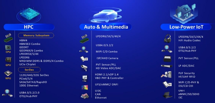
Figure 11: IP Offerings
Innosilicon Technology Inc.
97 E Brokaw Rd #210,
San Jose, CA 95112
For more information, contact sales@innosilicon.com