
Introduction
In the ever-evolving landscape of high-performance camera and display technologies, MIPI D-PHY™ and MIPI C-PHY™ specifications continue to lead the charge, setting benchmarks for low power, low latency, and high bandwidth data transmission. Building on the insights from our previous article, “Demystifying MIPI C-PHY/D–PHY Subsystem” – we now delve into the latest advancements in these specifications and their potential to transform vision and imaging technologies.
Market forces Driving New Features
When MIPI D-PHY was introduced over 15 years ago, its primary focus was on creating a simple, low power, and moderate bandwidth interface for the mobile market. In 2014, the introduction of MIPI C-PHY provided implementers with the option of operating over higher loss channels using a more energy efficient interface, albeit with some added complexity.
Since then, the industry has experienced an explosion in data rate requirements for cameras and displays due to increases in image dynamic range, pixel resolution, and frame rates. These enhancements are crucial not only for improving user visual experiences but also for enabling real-time advanced image processing. It’s no surprise then that a key feature of the MIPI D-PHY and MIPI C-PHY interfaces has been the continuous increase in maximum data rates across different versions to keep pace with market demands.
Recently, these interfaces have expanded beyond mobile markets, allowing companies to leverage economies of scale and investments in silicon design, software development, and testing infrastructure. Today, MIPI D-PHY and MIPI C-PHY are found in automotive (infotainment, advanced driver assistance systems, autonomous driving), industrial (machine vision, robotics, surveillance), immersive headsets (augmented reality/AR, virtual reality/VR, mixed reality/MR), healthcare, and other mobile influenced markets. Such a broad spectrum of applications is driving the evolution of the interfaces with an increased focus on power saving features, longer reach capabilities, reduced pin count, etc.
Deployment in these new markets also presents additional challenges for IP and IC vendors, which were not typically encountered in mobile applications. For instance, safety-critical applications in automotive require designs that accommodate larger sigma variations to reduce failure rates, incorporate safety mechanisms for fault detection, operate across broader junction temperature ranges, and ensure reliability over 10-15 years of operation. These new requirements are addressed by industry standards such as ISO26262, which focuses on functional safety, and AEC-Q100, which outlines stress testing for automotive-grade integrated circuits. Additionally, vendors must consider electromagnetic compatibility (EMC) to prevent high-speed data links from interfering with other electronic systems.
By remaining tuned to all these market forces and adapting the interfaces accordingly, MIPI D-PHY and MIPI C-PHY maintain their relevance as we transition into a new era of technological advancements in areas such as 6G, Artificial Intelligence (AI), and the Internet of Things (IoT).
MIPI D-PHY’s Newest Features
The older brother in the MIPI® short-reach physical interfaces family, MIPI D-PHY, was launched in 2009 and became an immediate success. It established the foundational framework for high-performance, low-cost connectivity for cameras and displays in mobile applications. The fundamental principles of the interface remained largely unchanged in the early versions of the standard. It maintained its source synchronous Double Data Rate (DDR) nature, featuring a High-Speed (HS) mode using SLVS differential signaling for high throughput data communication and a Low-Power (LP) mode using Spaced-One-Hot LVCMOS signaling for control purposes.
Data Rate Enhancement
Driven by the insatiable appetite for higher bandwidth, newer specification versions primarily focused on increasing the maximum bit rate per data lane—from 2500 Mbps in MIPI D-PHY v1.2 to 4500 Mbps in v2.x, and ultimately 9 Gbps in v3.x with the Standard Reference Channel. For shorter channel lengths, even higher rates are achievable, with up to 11 Gbps specified from v3.0 onwards, Understandably, the physical channel characteristics remained unchanged as the product form factors and physical distances to overcome were fundamentally the same. To support the increase in data rates, and mitigate the inherent higher signal losses and distortion, signal equalization features were introduced.
Equalization Options
In MIPI D-PHY v2.0, transmitter equalization was first defined in the form of signal de-emphasis, capable of boosting the High-Frequency (HF) to Low-Frequency (LF) signal ratio by 3.5 or 7dB for rates beyond 2.5 Gbps. In v3.0, with rates now up to 9-11 Gbps, Continuous Time Linear Equalization (CTLE), was also added on the receiver side to further enhance overall channel equalization. A combination of TX de-emphasis and RX CTLE is typically used to flatten the overall frequency response of the channel, including not just the interconnect but also package and silicon transceiver parasitic loads.
With the latest MIPI D-PHY v3.5, the use of non-linear Decision Feedback Equalization (DFE) was introduced in the receiver reference equalizer, suggesting that implementers could benefit in incorporating such techniques in actual receiver designs, particularly in those above 6 Gbps. Moreover, the standard does not prohibit the use of any of these techniques in designs conformant to earlier versions of the specification, allowing for backward compatibility and flexibility in implementation.
Low Power Features
New low power features have been introduced to enhance energy/bit efficiency while aligning the interface with advances in silicon processing technology and addressing modern day challenges. These features include:
- Half-swing mode: The High-Speed transmitter signal amplitude is halved, which is particularly useful for lower speed, short-reach connectivity.
- RX unterminated mode: The 100-ohm impedance is disabled on the receiver side (requires TX half-swing mode).
- Low Voltage Low Power (LVLP) mode: The Low-Power LVCMOS transmitter amplitude is reduced from a nominal 1.2V value to better adapt to core supplies in advanced CMOS processes.
When MIPI D-PHY originally adopted 1.2V LVCMOS signaling, such voltage levels were widely supported by most silicon technologies of the time. However, as more advanced process geometries emerged, several issues began to surface. Firstly, core supplies in these processes can be much lower than 1.2V (e.g., 0.75V in 5nm), requiring regulation from the I/O supply domain with all the drawbacks that carries. Secondly, 1.2V signaling can significantly overstress core devices in these processes, potentially increasing IO leakage and reducing device lifespan. Thirdly, rail-to-rail signaling of such high-levels severely restricts the length of supported channels. Finally, 1.2V signaling requires specific circuitry in both the transmitter and receiver sides, further reducing the maximum achievable speed due to increased load on the pad outputs.
LVLP was a transitional feature that addressed some of these issues by allowing LVCMOS signal levels to drop down to 0.95V. However, it couldn’t be scaled further without jeopardizing the correct differentiation between HS and LP signal levels. To tackle these challenges, MIPI D-PHY v2.5 introduced a new operational scheme known as Alternate Low-Power (ALP) mode. In this mode, LP signaling and its respective circuitry are no longer used; instead, its functions are ensured by the HS-TX and HS-RX circuitry used for high-speed communication. By using similar signal levels as in High-Speed mode, suitability, reliability, and excess leakage in advanced geometries are mitigated, while enabling operation over IoT channels of up to four meters.
Despite reusing HS-TX functions in ALP mode, there is a peculiarity where the HS-RX is unterminated during ALP signaling to save power, and the line levels are not always differential. This is illustrated in the figure below, where an ALP-00 state exists where both lines are grounded simultaneously.
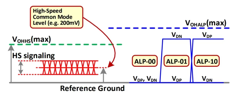
Figure 1: MIPI D-PHY Line Levels in HS and ALP Modes
ALP-00 serves as a direct replacement for legacy LP Stop and ULPS states. It is actively driven by the transmitter, grounding both lines to create a collapsed differential state with zero common mode and differential swing, which is key to power savings during extended periods of inactivity.
A generic burst format is illustrated in Figure 2, showing a clock lane and a representative data lane. Both lanes start in ALP Stop State (ALP-00), where they can remain for long periods of inactivity. When data or control information is ready for transmission, the clock lane wakes up first by sending an ALP-01 Wake pulse, followed by a similar Wake pulse on the data lane(s) once the forwarded high-speed clock is stable. The receiver link partner detects the ALP-01 Wake pulse using a special exit detector (ALP-ED), after which the differential termination is enabled in preparation for high-speed communication, which can include data, control codes, calibration patterns, and more.
The communication ends with the transmission of a long HS-Trail sequence (HS-1/ALP10) and a transition back to ALP Stop State, with the data lane(s) transitioning first, followed by the clock lane. The receiver on each lane detects the end of burst and disables the termination during the HS-Trail sequence. This entire process is repeated as needed to transmit additional data or control bursts.
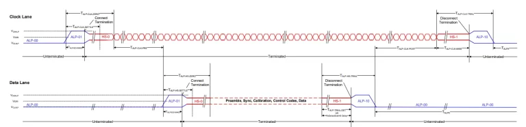
Figure 2: MIPI D-PHY ALP Mode Generic Burst
Another, perhaps less obvious but equally important, benefit of ALP is the reduction in lane turnaround time for applications using bidirectional lane modules. In LP mode, lane turnaround relies on a fixed pattern of Low Power states with a duration of 50ns, which does not scale with high-speed data rates. ALP introduces the concept of a Fast Lane Turnaround using a control burst with an embedded 16UI control code. At 1Gbps, this results in approximately half the turnaround time compared to legacy LP mode, with further reductions at higher operating rates. This effectively reduces turnaround times from over 1us in legacy LP mode to a few hundreds of nanoseconds in ALP mode.
The coordination of Fast Lane Turnaround and ALP features creates new use models for MIPI CSI-2® (Camera Serial Interface), enabling functionalities such as Unified Serial Link (USL). This innovation allows data communication and sideband Camera Control Interface (CCI) to be transported over the same high-speed link, reducing wire count and extending channel reach.
Forwarded clock interfaces such as MIPI D-PHY are prone to higher EMI emissions due to the presence of a continuous toggling clock. Although this can be somehow alleviated with system level shielding, MIPI D-PHY introduced spread spectrum capability starting from version 2.0. In this approach, the clock source frequency is typically modulated with a triangular profile, to spread the signal energy across a broader range of frequencies, thereby reducing peak emission levels at any given frequency. A down-spread profile is specified with a peak deviation of -5000ppm and a modulation rate between 30 and 33KHz.
Embedded Clock Mode
In May-2023, MIPI D-PHY v3.5 was introduced, featuring a new Embedded Clock Mode (ECM), marking a major shift in the D-PHY architecture. While the Forwarded Clock Mode (FCM) was retained for backward compatibility, ECM now embeds clock timing information in the data streams, which is then recovered on the receiver side with a Clock and Data Recovery (CDR) unit. This move brought several benefits:
- Reduction of EMI emissions: Suppression of the forwarded clock lane reduces electromagnetic interference.
- Relaxed skew alignment: Timing between lanes is now independent.
- Reduced wire count: A reduced 2-pin minimum configuration becomes possible.
- Increased data throughput: Repurposing the clock lane as a data lane increases total data throughput by 25%, assuming a typical 10 pin configuration (4 data + 1 clock) without increasing the data rate per lane.
Given the fundamental change to the original MIPI D-PHY operating framework, let us delve deeper into the new ECM mode and how it co-exists with FCM. Both modes are defined as optional in MIPI D-PHY v3.5, sharing the same interconnect and electrical specifications. This means a given PHY may support FCM, ECM or both. Effectively, v3.5 is the first version of MIPI D-PHY that does not absolutely guarantee backwards compatibility between Primary and Secondary devices – new v3.5 PHYs implementing only ECM will not be compatible with older v1.x-v3.0 PHYs. For PHYs supporting both ECM and FCM, there should be no dynamic transition between the two modes; only one mode is selected at initialization and remains selected throughout.
The shift from Forwarded to Embedded Clock Mode is accompanied by the deprecation or lack of support for some legacy features, including:
- High-Speed bidirectionality
- Alternate Low Power (ALP) mode
- Skew Calibration and FCM legacy preamble sequences
To embed the clock timing information into data streams, MIPI D-PHY ECM employs a 128b132b line encoding, like other industry standards, along with scrambling. Each 132-bit block is transmitted serially in the line (leftmost least significant bit first) with each block made up of 4-bit header and 128-bit payload. The header uses 4’b0011 for control and 4’b1100 for data, providing 1-bit error correction due to redundancy, resulting in a 3.125% overhead from coding.
Protocol data is scrambled using the polynomial G(x)=x23 + x21 + x16 + x8 + x6 + x2 + 1 and seed 0x1DBFBC, which is reset upon transmission of the Start of Packet (STP) control code. Any missing data from the protocol, to complete the 128-bit payload, is padded with zero-value bits.
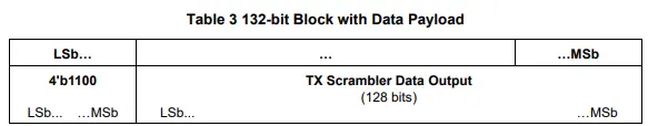
Figure 3: D-PHY ECM 132-bit Block with Data Payload
Control data is not scrambled, 32–bit control words are replicated four times (twice inverted and twice non-inverted) to complete the 128–bit payload while guaranteeing DC balance and error resilience.
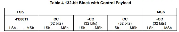
Figure 4: MIPI D-PHY ECM 132-bit Block with Control Payload
To avoid a gear-based interface, which would significantly increase costs in terms of PHY-Protocol buffering, D-PHY ECM defines a band-based interface with four possible operating bands. A Sensor/Display PHY may choose to implement a single band while an Application Processor (AP) PHY must implement all bands up to the highest supported band. A Transmitter only needs to support one data rate within a selected band, whereas a Receiver must operate at all rates within a supported band. These relationships ensure interoperability while keeping the overall cost of the system down.
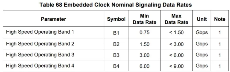
Figure 5: MIPI D-PHY ECM Operating Bands
Due to the band-based nature of the interface, a reference-less CDR may be used in every Secondary PHY instance. This unit locks onto the incoming bit stream at a rate within one of the four defined bands. This is important as it does not require the Secondary IC PHY to be pre-programmed to operate at a specific rate, thereby relaxing the requirements on PLL design. More importantly, it obviates the need for a local crystal reference, simplifying the overall design and reducing costs.
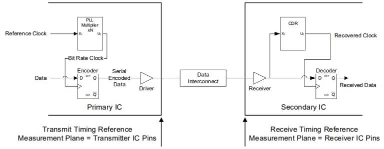
Figure 6: MIPI D-PHY ECM Timing Reference
A generic ECM burst sequence is shown in Figure 7, retaining many aspects and timings from FCM. The LP portions remain unchanged, with the most significant changes happening in the HS portion. The STP (Start of Packet) and EDP (End of Packet) delimit the encoded data, with an initial INIT-TRAIN sequence used to lock the CDR in the RX. The INIT -TRAIN sequence is 1010…, with an option for PRBS9 if EMI is a concern. Its duration is programmable to either short or long sequences, depending on the expected cumulative clock drift since the last burst transmission, which is specified not to exceed 25000ppm. As in FCM, there is no data throttling, so the PHY continuously transmits protocol data or control codes in high-speed mode, transitioning to LP-11 during long periods of inactivity. As the training sequences are quite long (thousands of UIs), frequent LP-HS-LP transitions, as done in the past with FCM, are less practical now. Therefore, the interface benefits from operating continuously in high-speed mode, with the protocol introducing filler/idle codes when no actual data is available for transmission.
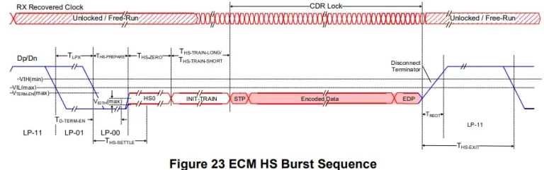
Figure 7: MIPI D-PHY ECM Generic Burst
By embedding clock timing within data streams, ECM enhances performance and simplifies design requirements, ensuring D-PHY remains a robust and adaptable solution.
Summary of MIPI D-PHY Features Evolution
The following table summarizes the main D-PHY features across specification versions.
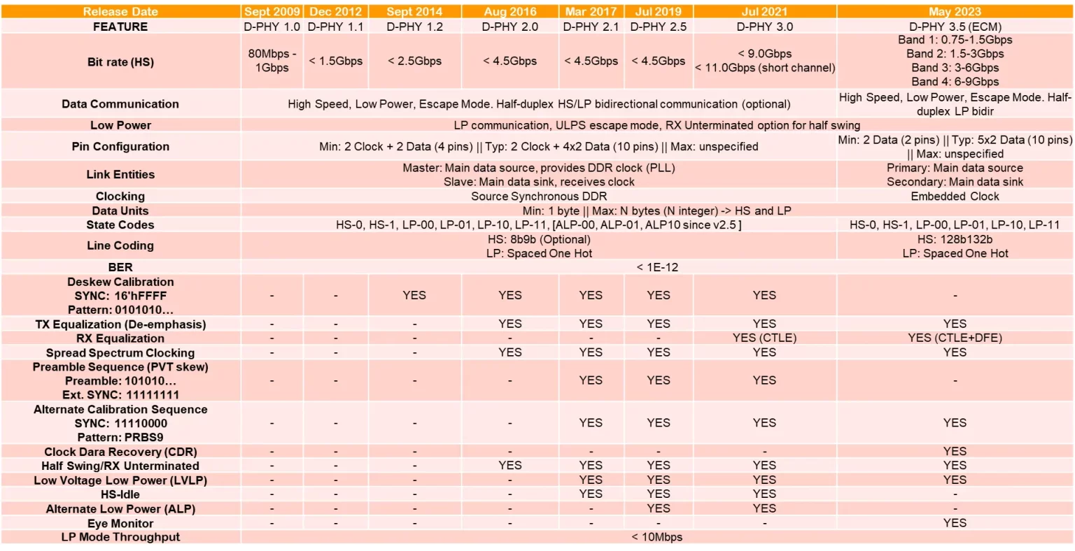
Figure 8: Summary of MIPI D-PHY Features
MIPI C-PHY’s Newest Features
It’s been over a decade since MIPI C-PHY v1.0 was released, and like MIPI D-PHY, there has been a push to increase its operating rates. Due to the multi-phase/level encoding used in MIPI C-PHY, where each symbol historically packed approximately 2.28 bits, the symbol rates have not increased as much as in MIPI D-PHY and yet, the total bandwidth for a similar pin count interface of the former consistently exceeds that of the latter.
Symbol Rate and Equalization Options
From the original 2.5 Giga Symbols per Second (Gsps) * 2.28 = 5.7 Gbps per lane rates, MIPI C-PHY evolved to 2.8 Gsps and 3.5 Gsps in versions 1.1 and 1.2, respectively. This was achieved with two different TX equalization schemes and special training sequences to fine-tune the receiver. Versions 2.x saw another increase in symbol rates, reaching 6 Gsps (~ 13.7Gbps/lane) for the Standard Reference Channel, through the addition of CTLE on the receiver side to better equalize the channel.
Low Power Features
On the low power front, MIPI C-PHY maintained alignment with MIPI D-PHY. In v1.1, the possibility of running RX without a termination at low speeds was introduced. From v1.2 onwards, new features were added: Low Voltage High Speed (LVHS) mode, where common mode and differential signal swing are reduced to better align with MIPI D-PHY levels (especially important for combo implementations); Low Voltage Low Power (LVLP) mode to reduce the LVCMOS levels; and finally, Alternate Low Power (ALP) mode.
ALP in MIPI C-PHY addresses the same problems previously described for MIPI D-PHY, yet the solution is somewhat different as it takes advantage of MIPI C-PHY reserved words for lane signalling events. The line levels are shown in Figure 9. There is some similarity with MIPI D-PHY, as the concepts of ALP-Pause and ALP Wake pulses are common, but with key differences: ALP Pause only requires VA=VB=VC, translating to a collapse of the differential swing for AB, BC, CA pairs but not necessarily implying grounded levels like in MIPI D-PHY. The Wake state is typically +X, where A line is high and B is low so that VAB = Vod_strong level, with C line at mid-level.
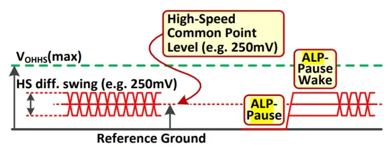
Figure 9: MIPI C-PHY Line Levels in HS and ALP Modes
A generic ALP burst format is shown in Figure 10 for a single data lane consisting of three wires (A, B, C). The lane always starts in ALP-Pause Stop (or ULPS) standby states, similar to legacy LP mode but using different line levels as explained before. The burst begins with the transmission of +X state for a sufficiently long period to wake up the remote receiver, which will typically be using a low-power detector to observe the state of the lines. Unlike MIPI D-PHY, there is no dynamic switching of the receiver side termination in MIPI C-PHY ALP mode, so weak and strong electrical levels remain consistent throughout the burst.
Following the +X Wake state, an all-1’s or all-3’s Preamble is sent, depending on whether ALP data/command burst or calibration burst is being transmitted. Regardless of the burst type, a final sequence consisting of a 7UI Stop or ULPS code followed by a programmable length POST2 field signals the receiver that the link will return to one of the standby states. This sequence provides sufficient trailing clock edges to process and flush the data upwards to the protocol.
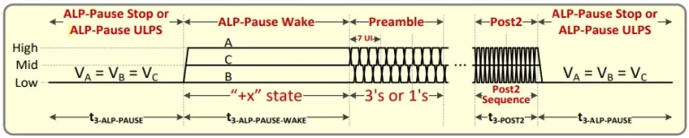
Figure 10: C-PHY ALP Mode Generic Burst Format
In between, High-Speed data or reserved Symbol sequences representing certain functions are sent to the link partner. One of these reserved sequences is the Turnaround Code (TAC), which initiates a Fast Lane Turnaround procedure where Primary side stops transmitting and moves to a receiving state while Secondary side moves to a complementary state. This procedure has similar benefits to those identified in MIPI D-PHY, specifically reducing latency of the operation compared with legacy LP Control Mode Lane Turnaround, as it is not constrained by the large LP state durations.
Unlike the MIPI D-PHY procedure, which requires a dedicated Control Burst, MIPI C-PHY utilizes its coding structure to embed a TAC code into the last data burst transmitted in the original orientation, further reducing the time needed to reverse the bus direction. Figure 11 below compares the Turnaround procedure in ALP mode versus the Legacy LP mode.
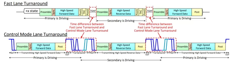
Figure 11: MIPI C-PHY Lane Turnaround Comparison
Data Rate Enhancement (18-Wirestate)
As the demand for increased bandwidth continues, MIPI C-PHY v3.0 was released in March-2025, featuring a completely new architecture based on the expansion to 18 wire states from the original 6 wire states. This change aims to increase MIPI C-PHY bit rates while maintaining or slightly reducing the symbol rates, operating over the same channels as earlier versions. Despite this fundamental shift in architecture, backward compatibility with older versions is maintained when operating in 6 phase mode.
So, what does this new architecture look like? How is the increase in bit rates achieved? Can it co-exist with the old one in an optimized way that reduces silicon costs? Let’s explore these questions by comparing both 6- and 18-Wirestate solutions.
Earlier versions of MIPI C-PHY mapped 16 bits of data from the controller into a group of 7 symbols, achieving an encoding gain of 16/7 = 2.28x. Six wire states were used for encoding (+X, -X, +Y, -Y, +Z, -Z), with each wire in a trio adopting one of three possible electrical levels (High, Middle, Low).
To boost bit rates while keeping the same symbol rates, the new 18-Wirestate mode maps 32 bits of data from the controller into a group of 9 symbols, achieving an encoding gain of 32/9 = 3.55x. There is no increase in physical resources at the interface, meaning the same three wires (trio) are used per lane. However, these wires now adopt one of seven possible signal levels creating 18 unique combinations of levels for AB, BC and CA differential pairs (WS0…WS17).
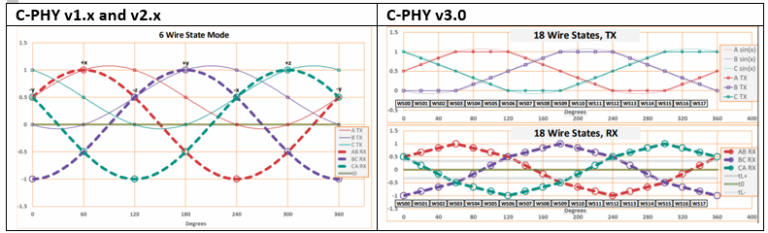
Figure 12: MIPI C-PHY 6- vs 18-Phase constellation
Figure 12 illustrates the difference in constellations for both solutions. In 6-Wirestate mode, only the polarity (+/-) of the AB, BC, and CA signal pairs needed to be determined for symbol detection. However, in 18-Wirestate mode, information is also encoded in the signal amplitude, requiring comparison against two additional amplitude thresholds (tL+ and tL-) to unequivocally identify each state. The receivers on each pair of lines are effectively multi-level slicers outputting one of four possible values.
To ensure at least one edge transition per symbol, MIPI C-PHY continuously moves between wire states, coding a total of 17 transitions. Mapping 32 bits into line symbols requires at least 232 ≈ 4.295×10⁹ unique combinations, which is far exceeded by a scheme offering 17 possible transitions for each of the 9 symbols used, yielding a total of 179 unique combinations. In practice, MIPI C-PHY v3.0 restricts the use of some symbols to reduce transition jitter and minimize the width of internal data paths, effectively becoming a base-12 system where 129 ≈ 5.15×10⁹ combinations are still sufficient to encode all possible 32-bit combinations.
The conversion between 32 bits and 9 symbols is achieved through a mapping function, with each symbol represented by a 5-bit code with 17 possible binary values (5’b00000-5’b10000). Each bit corresponds to a Wire state change parameter – Flip, Rotation, Polarity (F, R2, R1, R0, P) – like the 6-Wirestate mode:
- Polarity (lsb): Maintains the polarity of the wire state (1’b0) or changes it by 180° (1’b1).
- Rotation: Direction and amount of rotation in 2’s complement for [R2,R1,R0]:
- -1 to -4 for -40° to -160° rotation
- 0 to 3 for +40° to +160° rotation
- Flip (msb): Causes a 180° change in the next state (1’b1), with rotation and polarity ignored
The symbol information is captured in the transition between two consecutive wire states. Figure 13 illustrates this concept, where the 5’b01011 encoded symbol from the mapper leads to a transition from the present state WS02 to the next state WS05. The mapping function excludes symbols ‘0’, ‘7’, ‘9’, and ‘E’ due to higher induced jitter in recovered clock (these correspond to ±20° and ±40° rotations in the phase diagram). The ‘G’ symbol, corresponding to a 180° rotation or the Flip parameter, is also excluded. This exclusion simplifies implementation by reducing the symbol datapath from 45 to 36 bits.
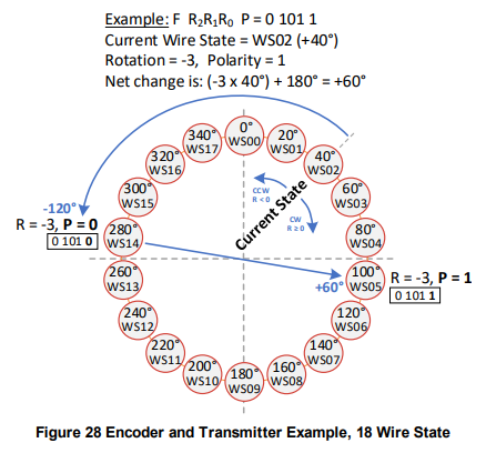
Figure 13: C-PHY 18-Wirestates Phase Diagram
Figure 14 illustrates the new (de–)mapping and (de)coding functions for 18-Wirestate mode.
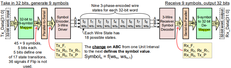
Figure 14: C-PHY 18-Wirestate Functions
From an electrical perspective, each wire in a trio is driven to one of seven equidistant electrical levels: LSL0 to LSL6. At any given time, all wires are at different levels, ensuring a non-zero voltage on all differential receivers and maintaining the same common voltage regardless of transmitted wire state (WS00 to WS17).
The 18-Wirestate line driver is a natural extension of the 6-Wirestate driver, incorporating six pull-up/down legs individually controlled by the pre-driver circuitry. Each leg has an output impedance six times higher than the nominal differential impedance and can easily generate the ‘high’, ‘low’, and ‘mid’ levels required in 6-Wirestate mode. There is no expectation that Transmitter De-emphasis is used in 18-Wirestate mode.
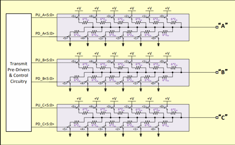
Figure 15: MIPI C-PHY 6-/18-Wirestate Line Driver
There are now ten differential levels at each receiver: four strong High, one weak High, four strong Low, and one weak Low). Additionally, there are three relevant eye diagrams (Upper, Middle, Lower) as shown in Figure 16. Unsurprisingly, the higher number of levels requires an increase in transmit power, with the VOD strongest levels now roughly doubling with respect to 6-Wirestate mode.
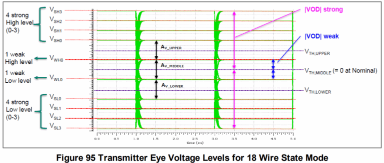
Figure 16: MIPI C-PHY 18-Wirestate Eye Diagram
Despite the various signal levels, each receiver only needs to differentiate between four different voltage ranges – Strong High, Weak High, Weak Low, and Strong Low – using three separate threshold levels to vertically slice the eye diagram and generating one of four possible outputs. Due to the reduction of Signal-to-Noise Ratio (SNR) from the multi-level signalling, the new receivers are specified to be twice as sensitive compared to the 6-Wirestate mode and are expected to always be used with an input CTLE to help compensate for channel induced Inter-Symbol Interference (ISI).
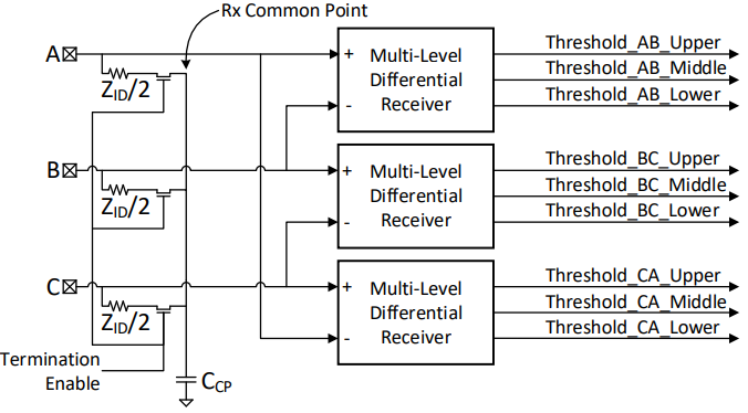
Figure 17: MIPI C-PHY 18-Wirestate Line Receiver
The latest MIPI C-PHY specification defines a maximum symbol rate of 5 Gsps, resulting in 5 * 3.55 = 17.75 Gbps per lane for the Standard Reference Channel when operating in 18-Wirestate mode. This far exceeds the 6 * 2.28 = 13.68 Gbps per lane throughput achievable in 6-Wirestate mode, even when operating with a higher symbol rate of 6 Gsps. The performance gap widens further when considering the Short Reference Channel: 18-Wirestate mode delivers up to 7 * 3.55 = 24.84 Gbps per lane, compared to 8 * 2.28 = 18.24 Gbps in 6-Wirestate mode.
Summary of MIPI C-PHY Features Evolution
The following table summarizes the main MIPI C-PHY features across specification versions.
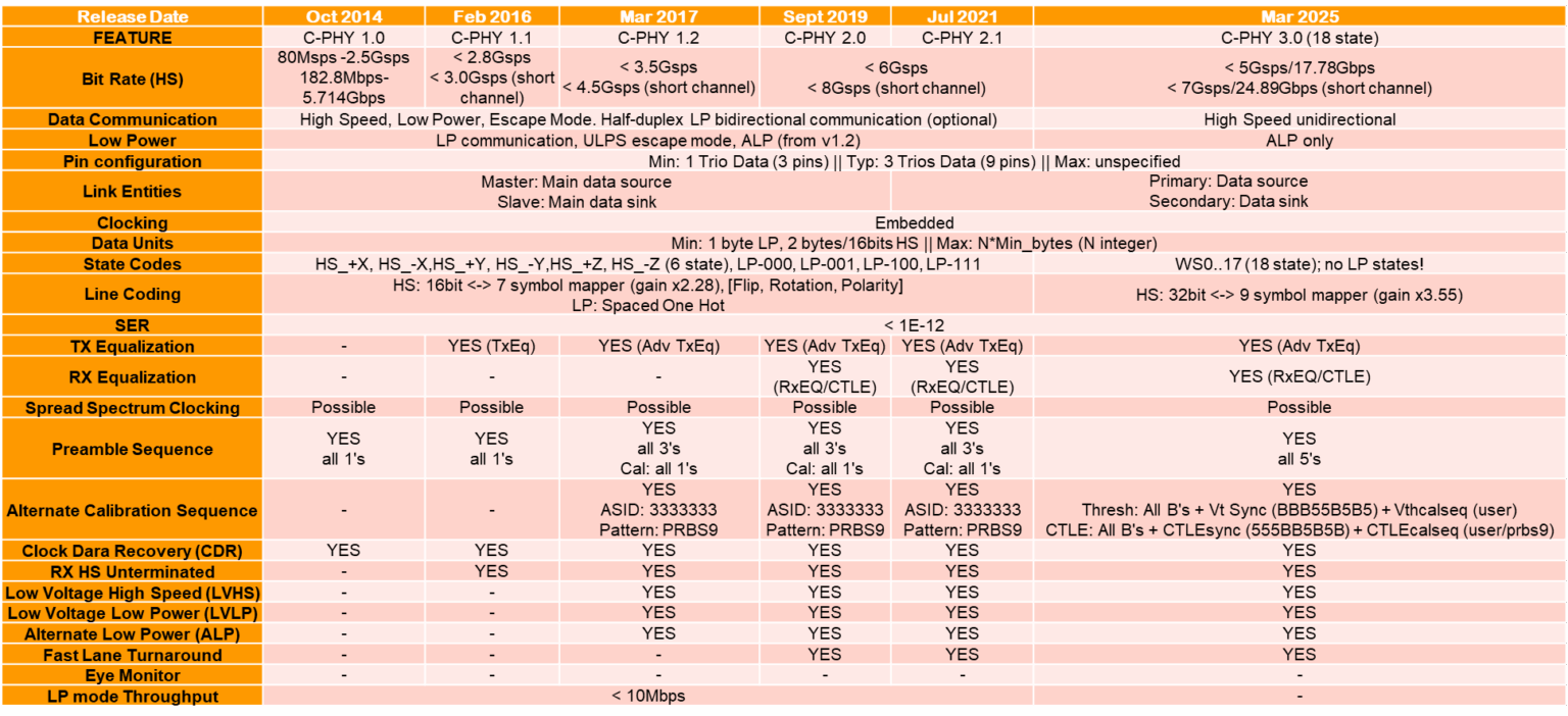
Figure 18: Summary of MIPI C-PHY Features
Conclusion
In summary, the advancements in MIPI D-PHY and MIPI C-PHY technology, including features such as Alternate Low Power (ALP) mode, Embedded Clock mode in MIPI D-PHY, and 18-Wirestate mode in MIPI C-PHY, effectively address critical challenges like compatibility with advanced process nodes, longer reach connectivity, wire count reduction, EMI emissions, and data throughput scalability. These innovations maintain efficient use of existing infrastructure and pave the way for newer, lower cost implementations while preserving backwards compatibility. As the technological landscape continues to evolve, the enhanced performance and flexibility of these interfaces will be pivotal in driving the next generation of high-speed communication systems for camera and display applications.
MIPI® is a registered trademark owned by MIPI Alliance. MIPI C-PHY™ and MIPI D-PHY™ are trademarks of MIPI Alliance.