
By Japesh Kumar – Senior Engineer, Qualcomm
Abstract
As semiconductor technology pushes the boundaries of scale and complexity, traditional VLSI physical design methodologies are struggling to keep pace. The rise of Artificial Intelligence (AI), particularly machine learning (ML) and deep learning (DL) offers a transformative opportunity to revolutionize physical design automation. This article explores how AI is being integrated across the VLSI physical design flow, from floorplanning to design rule checking, with real-world examples from industry leaders. We examine the tangible benefits, technical breakthroughs, and persistent challenges, and issue a call to action for engineers, researchers, and tool developers to embrace AI as a strategic enabler for next-generation chip design.
Keywords
VLSI, Physical Design, Artificial Intelligence, Machine Learning, Deep Learning, Floorplanning, Placement, Clock Tree Synthesis, Routing, Timing Closure, Design Rule Check, EDA
1. Introduction
The physical design phase in VLSI transforms digital logic into a manufacturable chip layout. As SoCs integrate more complex components from AI accelerators to high-speed interfaces, achieving optimal power, performance, and area (PPA) has become increasingly difficult.
Traditional EDA tools rely on heuristics and static algorithms, which struggle to scale with modern design complexity. AI introduces a data-driven, adaptive approach, capable of learning from vast design histories and optimizing across multiple objectives.
However, AI integration brings new challenges:
- Explainability: Designers need to understand AI decisions.
- Generalization: Models must work across diverse architectures.
- Trust: AI must complement, not replace, human expertise.
AI is reshaping physical design, but success depends on thoughtful integration and collaboration between engineers and intelligent tools.
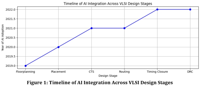
2. AI Across the Physical Design Flow
2.1 Floorplanning and Partitioning
Floorplanning is one of the earliest and most critical stages in the VLSI physical design flow. It defines the spatial arrangement of major functional blocks (macros, memory arrays, IP cores, etc.) on the silicon die. Partitioning, often done in tandem, involves dividing the design into manageable regions or clusters to optimize performance and layout efficiency.
Why It Matters
- Foundation for Layout: Decisions made during floorplanning directly affect placement, routing, timing, and power.
- Impact on PPA: Poor floorplanning can lead to longer interconnects, higher power consumption, and timing violations.
- Design Complexity: Modern SoCs contain billions of transistors and multiple subsystems, making manual floorplanning infeasible.
Key Objectives
- Minimize Wirelength: Shorter interconnects reduce delay and power.
- Reduce Congestion: Avoid routing bottlenecks by distributing blocks efficiently.
- Optimize Timing Paths: Place critical blocks close to each other.
- Thermal Management: Spread heat-generating blocks to avoid hotspots.
- Area Utilization: Maximize silicon usage while leaving room for routing and buffers.
AI Integration in Floorplanning
AI techniques are revolutionizing this stage by automating and optimizing decisions that previously required expert intuition:
Techniques Used
- Reinforcement Learning (RL): Models learn to place blocks by receiving feedback on wirelength, congestion, and timing.
- Generative Adversarial Networks (GANs): Generate diverse floorplan candidates that meet design constraints.
- Graph Neural Networks (GNNs): Model relationships between blocks and predict optimal placements.
Real-World Example
- Google’s AutoFloorplan: Used RL to optimize TPU chip layouts, achieving over 15% improvement in timing and reduced wirelength compared to traditional methods.
Challenges
- Generalization: AI models trained on one architecture may not perform well on others.
- Thermal and Manufacturability Awareness: AI must consider physical constraints beyond timing and area.
- Data Dependency: High-quality labeled data is essential for training robust models.
- Explainability: Designers need to understand why AI made certain decisions to trust and refine them.
Impact
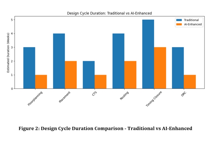
- Accelerated Design Cycles: AI reduces manual iterations and speeds up convergence.
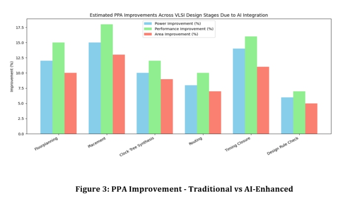
- Improved PPA Trade-offs: Smarter block placement leads to better overall chip performance.
- Scalability: AI can handle increasingly complex designs that challenge human capabilities.
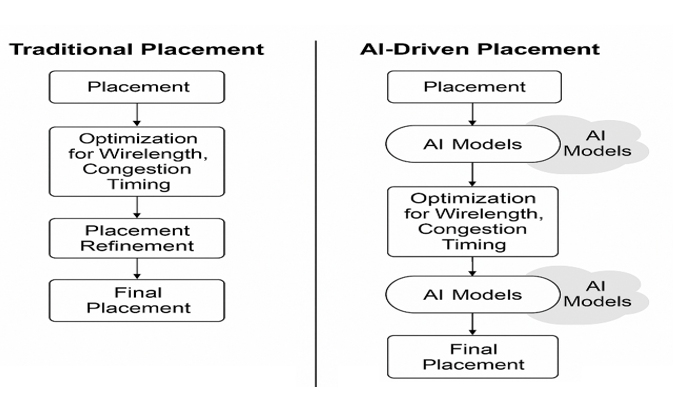
2.2 Placement Optimization
Placement optimization is a crucial stage in the VLSI physical design flow where standard cells (logic gates, flip-flops, etc.) are positioned within the predefined floorplan. The goal is to minimize wirelength, reduce congestion, and meet timing constraints all while ensuring manufacturability and power efficiency.
Why Placement Matters
- Direct Impact on Timing: Poor placement can lead to long interconnects, increased delay, and timing violations.
- Congestion Control: Efficient placement avoids routing bottlenecks and reduces the need for costly ECOs (Engineering Change Orders).
- Power Optimization: Shorter wires and better clustering reduce dynamic and leakage power.
- Design Scalability: With billions of transistors in modern chips, manual placement is impractical.
Objectives of Placement Optimization
- Minimize Total Wirelength
- Meet Setup and Hold Timing Constraints
- Avoid Routing Congestion
- Optimize Power Distribution
- Ensure Legal Placement (no overlaps, spacing rules)
AI Integration in Placement
AI is transforming placement from a heuristic-driven process to a data-driven optimization task.
Techniques Used
- Deep Reinforcement Learning (DRL): Learns optimal placement strategies by interacting with the design environment and receiving feedback on timing, congestion, and wirelength.
- Supervised Learning: Trains models on historical placement data to predict optimal cell positions.
- Graph Neural Networks (GNNs): Model the netlist as a graph and learn spatial relationships between cells.
Real-World Example
- NVIDIA’s AutoDMP: Uses DRL to automate placement, outperforming commercial tools in timing and congestion metrics. It reduced placement runtime by up to 50% while improving timing QoR.
Challenges in AI-Driven Placement
- Explainability: AI decisions are often opaque, making it hard for designers to debug or trust the results.
- Training Data Dependency: Models require diverse and high-quality datasets to generalize across designs.
- Scalability: Handling large-scale designs with millions of cells requires efficient model architectures.
- Integration with EDA Tools: Seamless interoperability with existing design flows is essential.
Impact of AI on Placement
- Accelerated Design Cycles: AI reduces iteration count and speeds up convergence.
- Improved Timing Closure: Smarter placement leads to fewer violations and better QoR.
- Enhanced Designer Productivity: Engineers can focus on higher-level optimization rather than manual tuning.
- Scalable Automation: AI can handle designs that are too complex for traditional methods.
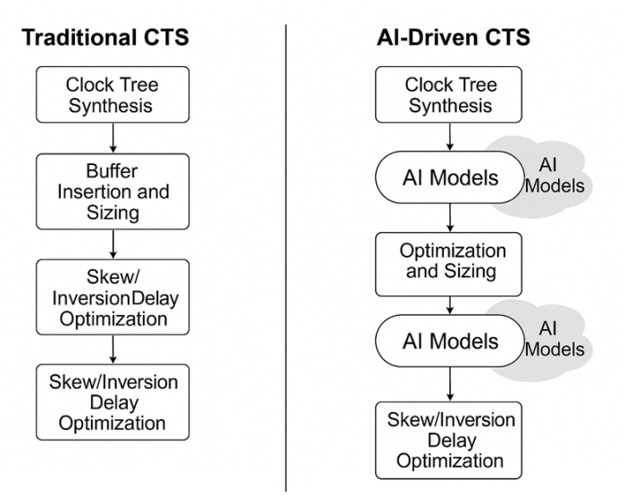
2.3 Clock Tree Synthesis (CTS)
Clock Tree Synthesis (CTS) is a critical stage in the physical design flow of VLSI chips. It involves designing the clock distribution network that ensures the clock signal reaches all sequential elements (like flip-flops) with minimal skew and insertion delay. A well-optimized clock tree is essential for achieving timing closure and maintaining signal integrity across the chip.
Why CTS Is Crucial
- Clock Skew Minimization: Ensures that all flip-flops receive the clock signal at nearly the same time, preventing setup and hold violations.
- Insertion Delay Control: Reduces the delay from the clock source to endpoints, improving timing margins.
- Power Efficiency: Optimizes buffer insertion and wire sizing to reduce dynamic power consumption.
- Signal Integrity: Prevents glitches and noise in the clock network that can cause functional errors.
Traditional CTS Workflow
- Clock Source Identification
- Clock Net Extraction
- Buffer Insertion and Sizing
- Tree Topology Generation
- Skew and Delay Optimization
- Validation and ECOs
AI Integration in CTS
AI is increasingly being used to automate and optimize CTS, especially in large-scale designs where manual tuning is impractical.
Techniques Used
- Predictive Models: Use historical design data to forecast optimal buffer locations and sizes.
- Topology Search Algorithms: AI evaluates multiple tree structures rapidly to find the best configuration.
- Reinforcement Learning: Learns placement strategies for clock buffers that minimize skew and power.
Real-World Example
- Cadence & Synopsys: Both EDA giants are integrating ML-based CTS engines into their tools. These engines predict buffer insertion strategies and optimize tree topologies, leading to reduced skew, lower power, and faster timing closure.
Challenges in AI-Driven CTS
- Corner-Case Coverage: AI models may miss rare timing violations, especially hold time issues.
- Data Dependency: Requires diverse and high-quality training data to generalize across designs.
- Black-Box Behavior: Lack of transparency in AI decisions can hinder debugging and trust.
- Integration Complexity: AI must work seamlessly with existing timing analysis and ECO tools.
Impact of AI on CTS
- Accelerated CTS Runtime: AI reduces the time needed to synthesize and validate clock trees.
- Improved Timing Robustness: Smarter buffer placement leads to better timing margins.
- Power Savings: AI can optimize buffer sizing and placement to reduce dynamic power.
- Design Scalability: Enables efficient CTS for large, complex SoCs.
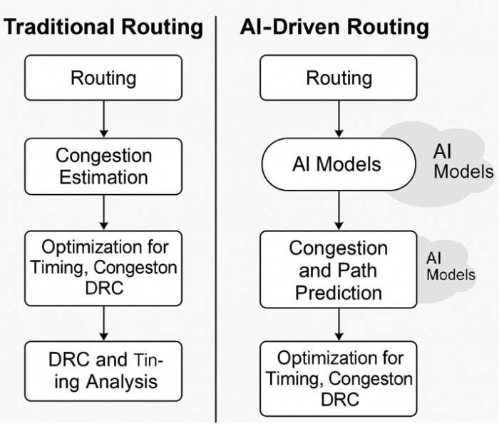
2.4 Routing
Routing is the stage in VLSI physical design where electrical connections are established between placed cells, macros, and I/O pins using metal layers. It transforms the logical netlist into physical wires while adhering to timing, power, and manufacturing constraints. Routing is typically divided into global routing (high-level path planning) and detailed routing (precise wire placement).
Why Routing Is Critical
- Timing Closure: Routing affects signal delays, which directly impact setup and hold timing.
- Congestion Management: Poor routing leads to bottlenecks, increasing the risk of DRC violations and ECOs.
- Manufacturability: Routed wires must comply with design rules to ensure yield and reliability.
- Power Integrity: Routing impacts IR drop and electromigration, especially in power and clock nets.
Traditional Routing Workflow
- Global Routing: Determines approximate paths for nets across routing regions.
- Detailed Routing: Assigns exact metal tracks and vias to each net.
- DRC and Timing Checks: Ensures routed nets meet physical and electrical constraints.
- ECOs: Fix violations and optimize critical paths.
AI Integration in Routing
AI is increasingly used to predict congestion, guide routing decisions, and reduce iteration cycles.
Techniques Used
- Neural Networks: Predict congestion hotspots and guide routing paths.
- Graph Search Algorithms: Model the routing grid as a graph and find optimal paths using learned heuristics.
- Reinforcement Learning (RL): Learns routing strategies by optimizing for timing, congestion, and DRC compliance.
Real-World Example
- Intel’s ML-Based Routing Predictors: Used internally to forecast congestion zones early in the flow, reducing ECO cycles and improving first-pass success rates.
Challenges in AI-Driven Routing
- Model Bias: AI may favor certain routing patterns that don’t generalize well across designs.
- Validation Complexity: AI-generated routes must be rigorously checked for DRC and timing violations.
- Integration with EDA Tools: AI must work seamlessly with existing signoff engines and rule decks.
- Scalability: Routing millions of nets across multiple layers requires efficient and scalable AI models.
Impact of AI on Routing
- Faster Routing Convergence: AI reduces the number of iterations needed to reach a valid solution.
- Improved First-Pass Success: Predictive models help avoid congestion and violations early.
- Reduced ECO Effort: Fewer late-stage fixes are needed, saving time and resources.
- Enhanced Design Quality: AI can optimize routing for better timing, power, and reliability.
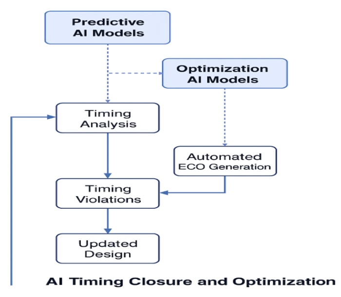
2.5 Timing Closure and Optimization
Timing closure is one of the most critical and challenging stages in the VLSI physical design flow. It ensures that all signal paths in the chip meet setup and hold timing constraints under worst-case conditions. Without timing closure, a chip may fail to operate reliably at its target frequency even if the layout is otherwise complete.
Why It Matters
- Functional correctness: Timing violations can cause incorrect data propagation, leading to chip failure.
- Performance targets: Timing closure determines whether the chip meets its intended clock speed.
- Tape-out readiness: A design cannot proceed to fabrication without passing timing checks.
Key Objectives
- Meet Setup and Hold Constraints: Ensure signals arrive within valid timing windows.
- Optimize Critical Paths: Shorten or buffer paths that violate timing.
- Balance Clock Skew and Insertion Delay: Coordinate timing across clock domains.
- Minimize ECOs (Engineering Change Orders): Reduce late-stage design modifications.
AI Integration in Timing Closure
AI is increasingly used to predict, analyze, and automate timing optimization tasks, especially in large designs where manual intervention is time-consuming.
Techniques Used
- Predictive Models: Forecast timing violations early in the flow using historical data and layout features.
- Automated ECO Engines: Suggest buffer insertions, gate sizing, or path restructuring to fix violations.
- Reinforcement Learning: Learn optimal timing fixes through iterative feedback.
Real-World Example
- IBM uses ML-based timing predictors to identify problematic paths and automate ECOs, reducing closure time by up to 30%.
- Cadence’s Tempus Timing Signoff Tool integrates AI to guide timing optimization decisions with higher accuracy.
Challenges
- Overreliance on AI: May obscure designer intuition, especially in edge cases.
- Explainability: Designers need to understand why a timing fix was suggested.
- Corner-case coverage: AI models may miss rare but critical timing scenarios.
- Data dependency: Requires diverse and high-quality training data to generalize across designs.
Impact
- Accelerated Closure Cycles: AI reduces the number of iterations needed to meet timing.
- Improved PPA: Smarter timing fixes lead to better performance without excessive area or power penalties.
- Reduced Manual Effort: Engineers can focus on strategic decisions rather than repetitive fixes.
2.6 Design Rule Check (DRC)
Design Rule Check (DRC) is the final gatekeeper in the physical design flow. It ensures that the layout adheres to the manufacturing constraints defined by the foundry. These rules are essential to guarantee that the chip can be fabricated reliably and will function correctly on silicon.
Why DRC Is Critical
- Manufacturability: Ensures that the layout can be produced using the target process technology.
- Yield Optimization: Prevents defects that could reduce the number of functional chips per wafer.
- First-Silicon Success: Minimizes costly re-spins by catching violations before tape-out.
Key DRC Checks Include
- Spacing Rules: Minimum distances between wires, vias, and transistors.
- Width Rules: Minimum and maximum widths of metal layers.
- Enclosure Rules: Proper enclosure of contacts and vias.
- Density Rules: Ensures uniform material distribution to avoid lithography issues.
AI Integration in DRC
AI is transforming DRC from a reactive verification step into a proactive prediction and prevention tool.
Techniques Used
- Convolutional Neural Networks (CNNs): Analyze layout patterns to predict violation-prone areas.
- Hybrid Systems: Combine rule-based engines with AI predictors for better accuracy.
- Transfer Learning: Apply learned violation patterns across different designs and nodes.
Real-World Example
- Google’s DeepDRC uses CNNs to scan layouts and predict potential violations before formal signoff, reducing runtime and improving first-silicon success rates.
Challenges
- False Positives/Negatives: AI models may incorrectly flag or miss violations.
- Data Requirements: Requires large, diverse datasets of annotated layouts.
- Integration Complexity: Must work seamlessly with existing rule-based DRC engines.
- Trust and Explainability: Designers need confidence in AI predictions, especially for critical paths.
Impact of AI on DRC
- Faster Signoff: AI reduces the time spent running exhaustive rule checks.
- Early Violation Detection: Identifies issues during placement and routing, not just at the end.
- Improved Yield: Helps avoid subtle layout issues that could impact manufacturability.
- Scalability: Handles increasingly complex designs with billions of transistors.
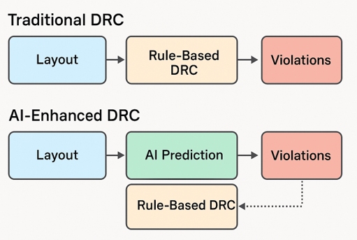
Design Rule Check (DRC): Traditional vs. AI Integration
Traditional DRC Workflow
DRC is a critical step that ensures the chip layout adheres to manufacturing constraints defined by the foundry. These rules cover:
- Minimum spacing between wires
- Via dimensions
- Layer overlaps
- Density requirements
Traditional DRC tools (e.g., Calibre, Pegasus) use:
- Rule-based engines: Hardcoded checks based on foundry specifications.
- Boolean operations: To detect violations in layout geometries.
- Batch processing: Often slow and resource-intensive, especially for large designs.
Limitations of Traditional DRC
- Long runtimes during signoff
- High memory usage
- Late detection of violations
- No predictive capability violations are found only after layout is complete
AI-Enhanced DRC Workflow
AI augments traditional DRC by introducing predictive and proactive capabilities:
AI Techniques Used
- Convolutional Neural Networks (CNNs): Analyze layout patterns to predict violation-prone areas.
- Graph Neural Networks (GNNs): Model spatial relationships between layout elements.
- Hybrid Models: Combine rule-based checks with ML predictions for higher accuracy.
Real-World Example
- Google’s DeepDRC: Uses CNNs to predict DRC violations before signoff, reducing runtime and improving first-silicon success.
- Synopsys DSO.ai: Integrates ML to guide layout decisions that minimize DRC violations.
Integration Workflow
|
Stage |
Traditional DRC |
AI Integration |
|
Pre-Layout |
No DRC |
AI predicts violation hotspots from floorplan |
|
During Placement/Routing |
Limited checks |
AI guides cell placement to avoid violations |
|
Post-Layout |
Full rule-based DRC |
AI pre-screens layout to reduce violations before signoff |
|
Signoff |
Final DRC run |
Hybrid DRC with AI + rule-based validation |
Challenges in AI-Driven DRC
- False Positives/Negatives: AI may misclassify due to limited training data.
- Generalization: Models trained on one technology node may not work on another.
- Trust and Explainability: Designers need confidence in AI predictions.
Benefits of Integration
- Faster DRC cycles
- Higher first-pass success
- Reduced ECOs
- Improved manufacturability
3. Comparative Summary
|
Design Stage |
AI Techniques Used |
Benefits of AI Integration |
Challenges and Limitations |
|
Floor Planning |
Reinforcement Learning (RL), Generative Adversarial Networks (GANs) |
Enables multi-objective optimization including wirelength, power, and timing; reduces manual iterations and improves layout quality. |
Limited generalization across architectures; lacks thermal and manufacturability awareness. |
|
Placement |
Deep Reinforcement Learning (DRL), Supervised Learning |
Accelerates convergence to optimal cell placement; improves timing and congestion metrics. |
Opaque decision-making; requires diverse training data for robust performance. |
|
Clock Tree Synthesis (CTS) |
Predictive Models, Topology Search Algorithms |
Optimizes clock skew and insertion delay; enhances timing robustness and power efficiency. |
May miss rare corner cases; dependent on comprehensive datasets. |
|
Routing |
Neural Networks, Graph Search Algorithms |
Predicts congestion zones and guides routing paths; improves first-pass success and reduces iteration count. |
Model bias and complexity; requires extensive validation across design styles. |
|
Timing Closure |
Predictive Analytics, Automated ECO Suggestion Engines |
Forecasts timing violations early; automates Engineering Change Orders (ECOs) to streamline closure. |
Risk of overreliance on AI; may obscure designer intuition and miss edge cases. |
|
Design Rule Check (DRC) |
Deep Learning Models, Hybrid Rule-Based + AI Systems |
Predicts violation-prone areas before signoff; accelerates DRC and improves first-silicon success. |
Requires large, diverse datasets; potential for false positives and negatives. |
4. Future Directions
The fusion of Artificial Intelligence (AI) and Electronic Design Automation (EDA) is not just a trend, it's a technological shift that is reshaping how chips are designed, optimized, and verified. As AI models become more powerful and design complexity continues to grow, several key directions are emerging that will define the next era of VLSI innovation:
1. Foundation Models for Chip Design
What it means:
Inspired by large language models like GPT, foundation models for chip design are pre-trained on massive datasets of layouts, timing paths, and design rules. These models can generalize across different process nodes, architectures, and design styles.
Why it matters:
- Reduces the need for retraining on every new design.
- Enables transfer of learning across domains (e.g., from mobile SoCs to data center chips).
- Accelerates design cycles by providing intelligent defaults and predictions.
Example:
Research efforts are underway to build transformer-based models that can predict timing violations or suggest placement strategies across diverse chip designs.
2. Self-Learning Design Flows
What it means:
AI systems that continuously learn from each design iteration adapting to new constraints, feedback, and outcomes without manual retraining.
Why it matters:
- Enables adaptive optimization as design evolves.
- Reduces human intervention in ECOs and late-stage fixes.
- Improves model robustness and accuracy over time.
Example:
An AI engine that learns from timing closure failures and automatically adjusts placement or buffering strategies in future runs.
3. AI + EDA Co-Design
What it means:
Instead of applying AI as a layer on top of existing EDA tools, co-design involves rethinking EDA algorithms and hardware together optimizing both for AI compatibility and performance.
Why it matters:
- Unlocks deeper integration between AI and physical design engines.
- Improves runtime, scalability, and accuracy.
- Enables hardware-aware AI models that consider silicon constraints.
Example:
EDA companies are exploring AI-native routing engines that work in tandem with GPU-accelerated solvers for real-time optimization.
4. Open-Source Acceleration
What it means:
Open-source projects are democratizing access to AI-driven design tools, enabling researchers and startups to experiment, contribute, and innovate without vendor lock-in.
Why it matters:
- Fosters transparency and reproducibility.
- Accelerates innovation through community collaboration.
- Lowers the barrier to entry for academic and emerging markets.
Examples:
- AutoDMP (NVIDIA): RL-based placement optimization.
- Triton (Google): Open-source compiler for AI workloads, influencing chip design.
- DeepDRC (Google): CNN-based DRC violation prediction.
5. Conclusion & Call to Action
Conclusion
Artificial Intelligence is no longer a theoretical enhancement in VLSI physical design, it is a practical, proven enabler of innovation. From Google’s AutoFloorplan to NVIDIA’s AutoDMP, and IBM’s predictive timing closure, AI is delivering measurable improvements in:
- Design cycle acceleration
- Power, performance, and area (PPA) optimization
- First-silicon success rates
However, AI is not a silver bullet. It must be integrated thoughtfully, with attention to model transparency, data diversity, and human oversight. The most effective design flows will be hybrid, combining the precision of AI with the intuition and experience of skilled engineers.
Call to Action
To fully realize the potential of AI in VLSI physical design, collaboration and proactive adoption are essential across the ecosystem:
- Chip Designers:
Begin exploring AI-enhanced tools in your workflows. Use predictive models to guide placement, timing, and DRC decisions. - Researchers:
Contribute to open benchmarks, interpretable models, and cross-node generalization techniques. Push the boundaries of AI explainability and robustness. - EDA Tool Developers:
Build interfaces that empower engineers do not replace them. Focus on transparency, configurability, and integration with existing design flows. - Foundries and IP Vendors:
Share anonymized design data to improve AI training and validation. Support open standards for AI-driven verification.
Why This Matters Now
As chips become more heterogeneous, power-sensitive, and performance-critical, traditional design flows are reaching their limits. AI offers a scalable, intelligent, and adaptive alternative but its success depends on how well we integrate it into the fabric of EDA.
The Future Is Smarter, Not Just Faster
AI is redefining what’s possible in chip design. But its success depends on us, the engineers, researchers, and innovators who shape the tools and workflows of tomorrow.
Let’s build the future of silicon together.
6. References
[1] Google Research, “Chip Design with Deep Reinforcement Learning,” 2021. [Online]. Available: https://research.google/blog/chip-design-with-deep-reinforcement-learning/
[2] NVIDIA Research, “AutoDMP: Automated DREAMPlace-Based Macro Placement,” 2023. [Online]. Available: https://research.nvidia.com/publication/2023-03_autodmp-automated-dreamplace-based-macro-placement
[3] Cadence, “Innovus CCOpt Clock Tree Synthesis,” [Online]. Available: https://www.cadence.com/en_US/home/training/all-courses/86198.html
[4] Synopsys, “DSO.ai – AI-Powered EDA Optimization,” [Online]. Available: https://www.synopsys.com/ai/ai-powered-eda/dso-ai.html
[5] IBM Research, “ML-Driven SoC Design Optimization,” [Online]. Available: https://research.ibm.com/publications/cloud-bursting-an-eda-workload-with-ml-driven-technique-for-future-soc-development
[6] Google Research, “Controlling Neural Networks with Rule Representations,” [Online]. Available: https://research.google/blog/controlling-neural-networks-with-rule-representations/
[7] IRJET, “Artificial Intelligence in VLSI Physical Design,” 2024. [Online]. Available: https://www.irjet.net/archives/V11/i10/IRJET-V11I1039.pdf
[8] ChipXpert, “Top 10 Open-Source VLSI Tools,” 2025. [Online]. Available: https://chipxpert.in/10-must-try-open-source-tools-for-every-vlsi-student-in-2025/
[9] SpringerLink, “Design Space Exploration in VLSI Using Machine Learning,” [Online]. Available: https://link.springer.com/chapter/10.1007/978-981-97-8043-3_194
[10] SpringerLink, “Machine Learning Techniques for VLSI Circuit Design: A Review,” [Online]. Available: https://link.springer.com/chapter/10.1007/978-3-031-64847-2_17
[11] arXiv, “AI/ML Algorithms and Applications in VLSI Design and Technology,” [Online]. Available: https://arxiv.org/pdf/2202.10015
[12] arXiv, “Benchmarking End-to-End Performance of AI-Based Chip Placement Algorithms,” [Online]. Available: https://arxiv.org/html/2407.15026v1
[13] arXiv, “A Survey of Circuit Foundation Models for VLSI Design,” [Online]. Available: https://arxiv.org/abs/2504.03711
[14] arXiv, “Towards Machine Learning for Placement and Routing in Chip Design,” [Online]. Available: https://arxiv.org/pdf/2202.13564
[15] arXiv, “FloorSet – VLSI Floorplanning Dataset,” [Online]. Available: https://arxiv.org/abs/2405.05480
[16] GitHub, “FloorSet Dataset Repository,” [Online]. Available: https://github.com/IntelLabs/FloorSet
[17] GitHub, “CircuitNet Dataset Repository,” [Online]. Available: https://github.com/circuitnet/CircuitNet
[18] CircuitNet, “Project Website,” [Online]. Available: https://circuitnet.github.io/
[19] GitHub, “EDA Corpus for LLM Training,” [Online]. Available: https://github.com/OpenROAD-Assistant/EDA-Corpus
[20] arXiv, “ChiPBench Benchmark,” [Online]. Available: https://arxiv.org/abs/2407.15026
[21] ACM Digital Library, “EDA-Schema Dataset,” [Online]. Available: https://dl.acm.org/doi/fullHtml/10.1145/3649476.3658718