
SUSTAINABLE AI GROWTH AND ENERGY CONSUMPTION: THE KEY EQUATION TO SOLVE!
Artificial intelligence (AI) has become a transformative force across various industries, driving innovation and efficiency, but it's crucial to consider the sustainability of these advancements to ensure long-term benefits for society and the environment.
Sustainable AI growth involves addressing several key challenges, with energy consumption being one of the main problems to solve. AI large language models (LLMs) require rapid processing of large datasets, which demands significant computational power and leads to high energy consumption. Recent comments from industry executives anticipate, on the compute side, a factor of 100 times more computes required for the next generation of LLM training while on the power side, the energy needed to train a leading model is multiplied by 10 every two years.
Partitioning processing over accelerators are driving key parameters needs
The processing of LLMs is typically partitioned over different accelerators to optimize performance. Accelerators communicate with each other to pass intermediate results. Large local accelerator clusters need energy-efficient, high-speed, low-latency, dense interconnects that can scale, and the pressure to improve these figures of merit will continue to increase.
The limitations of electrical interconnects call for a new generation of optical links
As data rates increase, the reach of pure electrical links becomes shorter. The reach can be extended by replacing the direct attach copper (DAC) cable with an active electrical cable (AEC) that integrate retimers; although this comes at the expense of energy efficiency and added latency. Optical interconnects which use light to transmit data, experience less degradation over distance and travel faster than traditional electrical signals. This results in lower latency and lower power consumption for data communications between different parts of the AI cluster.
Silicon photonics is the path for pluggable optics large volume energy-efficient links
Silicon photonic integrated circuits (PICs) based on silicon photonics integrate multiple photonic functions, such as light generation, modulation, and photo detection, onto a single chip. This integration consolidates all the functions of an optical transceiver into a single die, offering several advantages over traditional discrete photonic components, including:
- Smaller footprint (>0.5 Tbps/mm²)
- Higher integration density (>1 Tbps/mm)
- Improved yields and reliability thanks to mature semiconductor manufacturing process by leveraging CMOS 300 mm manufacturing facilities (<0.1 $/Gbps), compared to traditional 200 mm plants
- Significant reductions in power consumption (<5 pJ/bit)
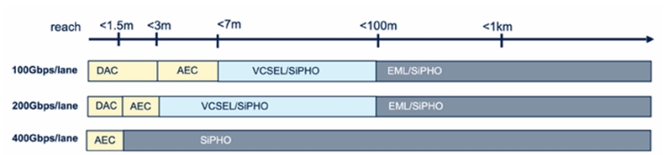
Figure 1: Silicon photonics is the best technology for enhanced performances short and long fiber length
A new class of products is emerging: optical chiplets for chip-to-chip communication
While the industry has made significant strides in enhancing the energy efficiency of pluggable optical modules (LPO/LRO), the specific requirements of GPU-to-GPU local network demand even more efficient optical interconnect. Silicon photonics-based transceivers offer significant potential for improving the efficiency of data transfer within local GPU accelerators. By integrating electrical and photonic integrated circuits (PICs) in a 2.5D package, these transceivers can facilitate die-to-die communication with the GPU through very low power and parallel dense electrical interfaces. This approach, often referred to as an optical chiplet, can significantly increase energy savings for large data transfers by removing copper connections, making it a crucial technology for the future of high-performance computing and data centers.
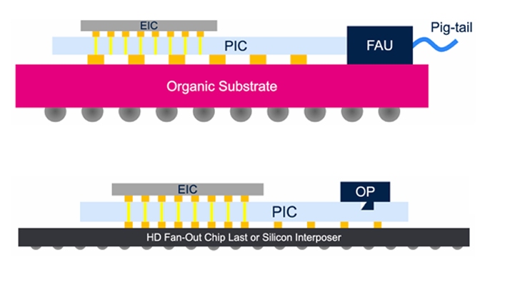
Figure 2: Silicon photonics is the best technology for compact and power efficient optical chiplets on classical organic substrate or more advanced silicon interposer
STMICROELECTRONICS LEADING-EDGE SILICON PHOTONIC PLATFORM: PIC100
Silicon photonic PIC100 technology represents a cutting-edge advancement in the field of optical communications and integrated photonics. Silicon photonics leverages the well-established silicon manufacturing infrastructure to create photonic integrated circuits (PICs) that can manipulate light for high-speed data transmission and processing.
STMicroelectronics already has extensive experience in Si-Photonics research, development, and industrialization [3-6], and was a pioneer in introducing its first 300 mm silicon photonic platform (PIC25G) in 2013 [3]. This platform achieved 25 Gbaud per lane to reach 100 Gbits/s with 4 fibers and NRZ signals, utilizing 35GHz bandwidth modulators and photo-diodes, using only silicon waveguides. At that time, the demand was limited and not sufficient to maintain a production activity scaled for large volume. However, the teams maintain an active R&D presence in the optical ecosystem, driven by the belief in a more promising future market. AI is now the game changer.
In 2025, leveraging this experience and continuous R&D we introduce our next silicon photonics PIC100 platform for 200 Gbps/lane PAM4 (100 Gbaud), which represents a leading-edge advancement in the field of optical communications and integrated photonics.
Compared to our previous PIC25 platform, we optimized the Si waveguide process to reduce single-mode waveguide optical losses down to 0.4 dB/cm. SiN waveguides are also available to ease fiber coupling and propose low-loss passive functions, with optical losses as low as 0.5 dB/cm for 1310 nm and 1550 nm wavelengths using adapted materials. Compared to the industry's best known performance today (0.8 dB/cm), these achievements are best-in-class for 300 mm.
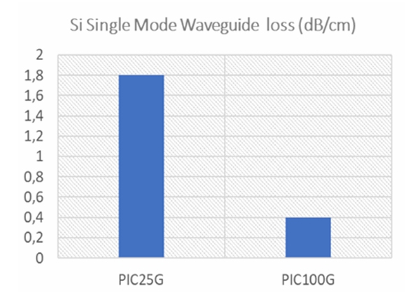
Figure 3: Improvement in Si single-mode waveguide losses (dB/cm) compared to previous technology
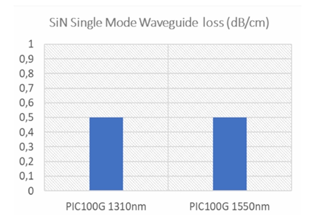
Figure 4: SiN single-mode waveguide losses (dB/cm) for 1310nm and 1550nm wavelengths
Regarding the HSPM (high-speed phase-shift modulator), we improved light confinement in the core of the waveguide (Figure 5), maximizing the modal overlap with the PN junction. This improves the modulator efficiency (VpiLpi) by a factor of 2 compared to our previous platform (Figure 6).
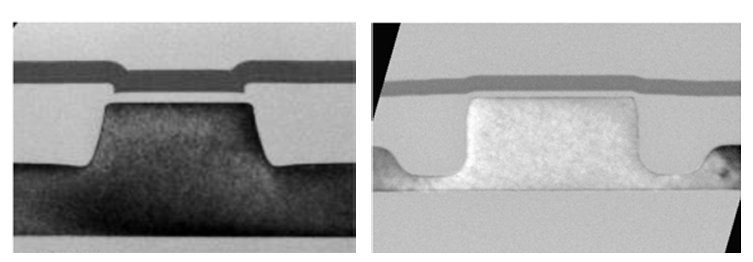
Figure 5: (top) PIC25G HSPM and (bottom) PIC100G HSPM cross section, showing the new device structure.
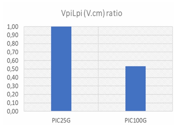
Figure 6: Ratio of VpiLpi between PIC25G HSPM and PIC100G HSPM. The performance is improved by a factor 2.
The different doping schemes and structure of the modulator arms have been fully optimized to drastically reduce the access resistance of the modulator, as well as the doping profile in the waveguide to optimize the capacitance vs. optical phase shift efficiency. Both optimizations allow an R*C product reduction by 2/3 (Figure 7) and a maximum modulation frequency improved by a factor of more than 2 compared to our previous technology (Figure 8).
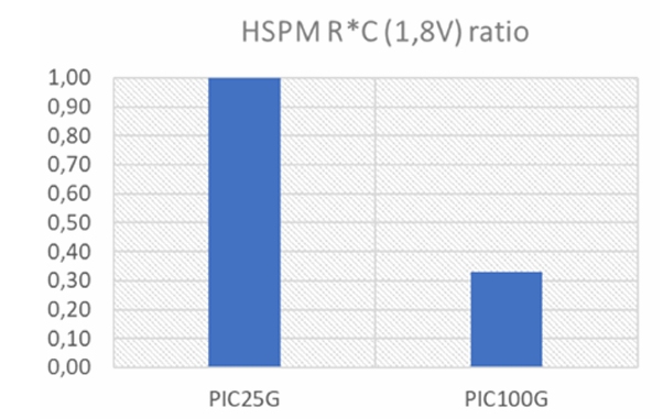
Figure 7: Ratio of the Product R (total access resistance) and C (HSPM device capacitance) between PIC25G HSPM and PIC100G HSPM. The structure has been optimized to drastically reduce R*C to improve speed.
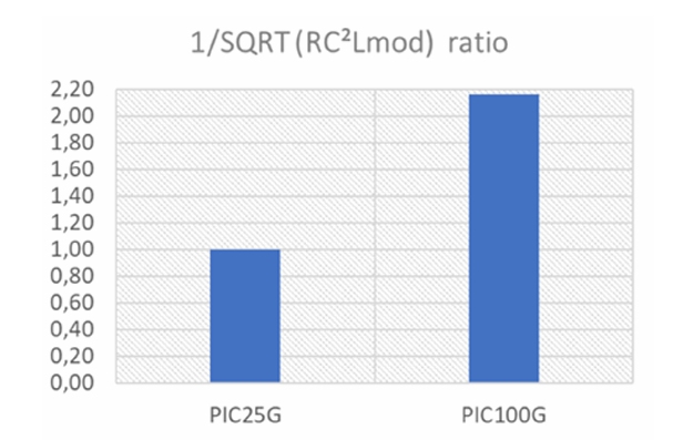
Figure 8: Ratio of our Figure of Merit (1/√RC².Lmodulator) between PIC25G HSPM and PIC100G HSPM. The modulator length is adapted for an Extinction Ratio of 4.5dB. This figure of merit is directly proportional to the electro-optical bandwidth of the modulator, showing that our PIC100G speed is more than 2 times that of our previous PIC25G industrial platform.
Regarding low-speed modulation, the PIC100 technology introduces a thermal phase shifter using a TiN layer. On the receiver side, a new generation of Ge photodetector has been developed with cut-off frequencies above 80 GHz at -1V, surpassing the industry's best known performance of 70 GHz.
Finally, optical I/O relies on edge coupling. Thanks to an innovative thick process stack and SiN waveguide layer, the typical fiber to guide coupling performance is <1.5 dB, when tested on wafer.
In conclusion, the integration of state-of-the-art devices such as Si and SiN waveguides, high-speed phase modulators, high-speed photodiodes, and edge couplers into a patented, innovative 300 mm stack is unique in the market. This enables the new generation of 800 Gbps and 1.6 Tbps pluggable optics
ST BICMOS B55/B55X: SPEED, GAIN, AND LINEARITY ALL IN ONE!
Silicon Germanium (SiGe) BiCMOS has a long track record of serving high-speed optical interconnect applications since the start of the Ethernet Gb/s era. It is considered the best technology for developing companion electronics ICs. These ICs, including TIA modulators, laser drivers, and clock and data recovery units, combine analog ICs that operate at frequencies as high as the bit rate to stream high-speed data with minimal distortion and jitter generation. They also incorporate high-speed digital logic for multiplexing and de-multiplexing functions [CHEN2001].
The unique characteristics of SiGe BiCMOS technology allow for the fabrication of cost-effective, high-performance, and low power ICs.
SiGe BiCMOS technology relies on three pillars:
- SiGe Heterojunction Bipolar Transistors (HBT),
- RF passive devices,
- CMOS transistors.
Fig. 9 illustrates the co-integration of these pillars in a 55-nm CMOS node [CHEVALIER2014].
As shown in Fig. 10, it has been accompanied by a multiplication by ~8 of the peak of both the current gain transition frequency fT and the maximum oscillation frequency fMAX of SiGe HBT, reaching today 385 GHz fT and 500 GHz fMAX [GAUTHIER2023, CHEVALIER2024B]. This is key to increase the baud rate and allows targeting 100 Gbaud with technologies in production today [TORFS2023]. Indeed, although higher-order optical modulation is very effective to increase the wavelength capacity, higher baud rates are important for reducing cost per bit, power, and footprint [INFINERA_WHITE_PAPER]. Finally, the quality of passive devices, i.e., resistors, capacitors, varactors, inductors, and transmission lines, is of utmost importance to design best-in-class circuits. Performance of inductors and transmission lines being driven by the coupling with the substrate, high-resistivity substrates and / or ultra-thick metallization stack are proposed. Ultra-thick copper metal lines are also able to drive more current.
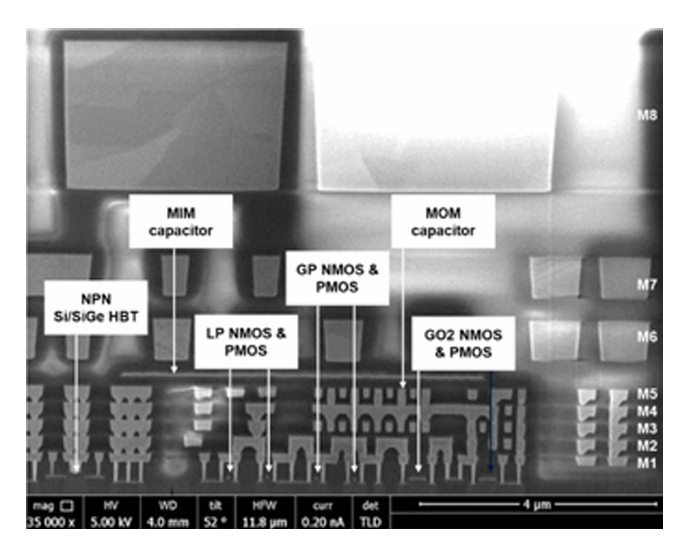
Fig. 9: SEM cross section of a 55-nm SiGe BiCMOS technology [CHEVALIER2014] showing the primary devices and BEOL up to Metal 8 with the SiGe base layer highlighted. MIM: metal insulator–metal; MOM: metal–oxide–metal; BEOL: back-end of line; NPN: N-type emitter, P-type base, N-type collector; LP: low power; GP: general purpose; GO2: second (thick) gate oxide.
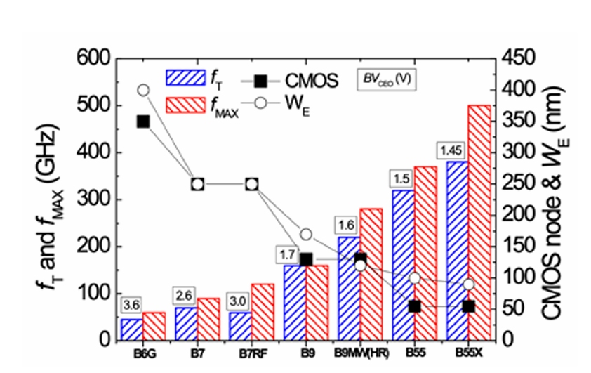
Fig. 10: STMicroelectronics high-speed SiGe BiCMOS technologies (HBT performance & CMOS node). WE is the physical emitter width. BVCEO is the emitter collector breakdown voltage of the HBT with an open base. fT and fMAX correspond to the peak values measured for the SiGe HBT. [From [CHEVALIER2024A]].
Last SiGe BiCMOS technology released by STMicroelectronics, BiCMOS055X (so called B55X) has been designed to cover a wide range of applications, which includes high-speed optical communications. B55X is the 2nd BiCMOS generation in STMicroelectronics being based on a 55-nm CMOS node. The masterpiece of this technology is the 4th generation of high speed SiGe HBT featuring an epitaxial extrinsic-to-intrinsic base link (cf. Fig. 11.a), which is key to reduce the base resistance and get low noise and high fMAX . This transistor exhibits at VBE = 0.7 V a current gain b ~2000 and a collector-to-emitter breakdown voltage BVCEO = 1.45 V. Fig. 12 shows peak fT between 360 and 400 GHz and peak fMAX between 450 and 500 GHz, depending on the emitter length, are extrapolated from measurements up to 110 GHz. Metallization stacks differentiate by the number of thin and thick levels, offering a trade-off between digital performance and process complexity / cost. Indeed, thanks to the dual ultra-thick copper module featuring lines and vias thicknesses of 2.3 µm and 2.7 µm respectively, RF performance is barely impacted by the choice of the stack. For example, the Q-factor of a 300pH single-ended inductor at 20 GHz only reduces from 30.2 to 28.8 between a 9ML Cu and a 6ML Cu stack [CHEVALIER24B]. An optional 5 fF/µm² Metal-Insulator Metal (MIM) capacitor is also available. Contrary to the previous generation (B55, [CHEVALIER2014]), 3 families of MOS transistors (corresponding to the 3 gate oxide thicknesses) can be selected separately in 4, fully compatible, gate oxide (GO) options [CHEVALIER24A, CHEVALIER24B].
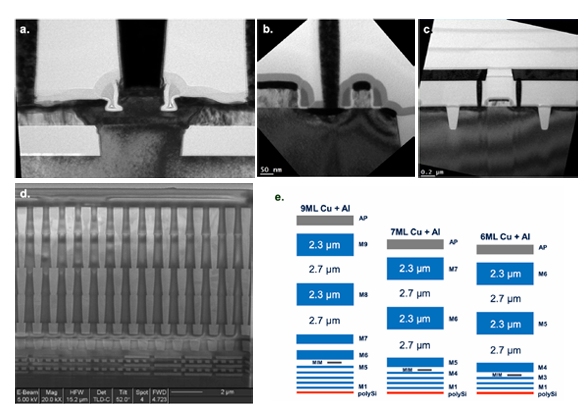
Fig. 11. TEM cross-sections: SiGe HBT (a), 1.8-nm thick oxide MOS (b), 5-nm thick oxide MOS (c) | 9ML Cu BEOL SEM cross-section (d) | 9ML, 7ML and 6ML Cu BEOL schematic representations (e) (From [CHEVALIER 24B]).
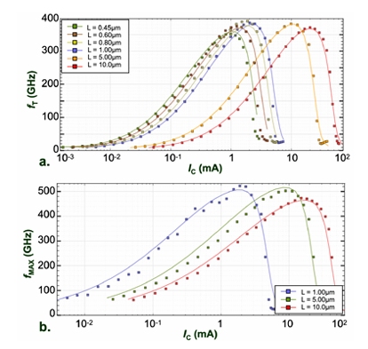
Fig. 12. High-speed SiGe HBT (without DTI) fT (a) and fMAX (b) vs. IC for different (drawn) emitter lengths (0.45 to 10 µm) at VCB = 0.3 V and T=25°C: comparison between measurements (dots) and model (lines), (from [CHEVALIER24B]).
The superiority of SiGe BiCMOS over CMOS for applications above 100 GHz has been reported for a long time. Beyond its excellent noise performance, which is highly valued for TIAs, power amplifiers (PAs) using SiGe HBTs surpass those fabricated in CMOS [VOINIGESCU2017].
While the feasibility of 100 Gbaud PAM4 modulation per wavelength to support 4-lane 800Gb/s and 8-lane 1.6Tb/s Ethernet has been demonstrated in B55 [TORFS2023], B55X provides more bandwidth, that can either be used for larger data rate (+100 Gbaud) or traded against lower power and/or more design margin. B55X capability is illustrated by the results simulated for a 224Gb/s PAM4 receiver chain (RX) shown in Fig. 13. Simulations show a 60 GHz bandwidth (cf. Fig. 14) together with a 0.75 pJ/bit power consumption. Finally, the 3D-assembly of BiCMOS ASICs onto a silicon photonics front-end IC using copper pillars is a powerful combination that has been demonstrated with B55+PIC25G [TEMPORITI2016, SENTIERI2020].
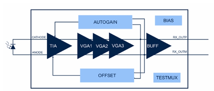
Fig. 13. 224Gb/s PAM4 receiver (RX) architecture simulated in B55X.
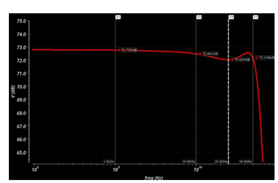
Fig. 14. Simulated electrical frequency response of the RX TIA gain ZT of Fig. 5
B55X AND PIC100 THE WINNING TECHNOLOGIES FOR OPTICAL ENGINES
The need of power-efficiency dramatically stimulates the packaging ecosystem. STMicroelectronics is currently qualifying the micro-bumping process on PIC100 and on B55X, to answer this problematic right now for 800 Gbps and 1.6 Tbps applications. This offers several benefits:
- High-integration density at optimized cost and maximized performance: By stacking components vertically, the overall footprint of the chip is significantly controlled, allowing for compact designs. This approach enables optimized fabrication on separate processes, reducing complexity compared to a single-process fabrication, while still achieving monolithic integration of EIC and PIC functions on a single die.
- Enhanced bandwidth performance to address 400 Gbps/lane: shorter interconnects between stacked layers minimize signal loss, improving overall signal integrity, enabling the path to the electrical optical conversion @ 400 Gbps per lane.
The TSV 40µm minimum pitch, under development in this 300 mm platform, will also enable the die-to-die communication within the same package of the Host (GPU or Switch) through parallel dense interface (like UCIe-A, 2mm interconnect lengths, 0.25 pJ/ bit) improving the overall power efficiency of the system.
Finally, as AI models continue to grow in complexity and size, the demand for efficient data transfer and processing will increase. ST PIC100 Silicon photonics and BiCMOS B55X provides a future-proof solution for 800G and 1.6Tbps pluggable optics, paving the road to a long-term roadmap including xPU-x optical interconnects, ensuring that AI clusters growth remain sustainable and efficient.
In conclusion, STMicroelectronics' PIC100 silicon photonics and BiCMOS B55X technologies provide cutting-edge solutions for 800G and 1.6Tbps pluggable optics, ensuring sustainable and efficient AI cluster growth. These advancements enable high integration density, enhanced bandwidth performance, and significant power efficiency, paving the way for future AI optical interconnects.
THE FOLLOWING ST PEOPLE CONTRIBUTED TO THE WRITING OF THIS DOCUMENT:
- Frederic Boeuf - Technical Director, Photonics Innovations & ST Fellow
- Pascal Chevalier - Technical Director, Technology Architecture & ST Fellow
- Sébastien Cremer - Silicon Photonics Technology Manager
- Sabina Fanfoni - Senior Product Marketing Manager, Silicon Photonics
- Lorenzo Gerosa - Senior Principal Engineer
- David Jacquet - System Architect & ST Fellow
- Stephane Monfray - Senior Principal Engineer
ADDITIONAL RESOURCES
Bipolar CMOS (BiCMOS) semiconductor technology [ST technology page]
Silicon photonics (SiPho) technology [ST technology page]
STMicroelectronics to enable higher-performance cloud optical interconnect in datacenters and AI clusters [Press release]
PIC100: ST’s 1st silicon photonics technology offers performance, efficiency, and a vision of what the future looks like in data centers [Webpage]
REFERENCES
- F. Boeuf et al., "A multi-wavelength 3D-compatible silicon photonics platform on 300mm SOI wafers for 25Gb/s applications," 2013 IEEE International Electron Devices Meeting, Washington, DC, USA, 2013, pp. 13.3.1-13.3.4, doi: 10.1109/IEDM.2013.6724623.
- F. Boeuf et al., "A Silicon Photonics Technology for 400 Gbit/s Applications," 2019 IEEE International Electron Devices Meeting (IEDM), San Francisco, CA, USA, 2019, pp. 33.1.1-33.1.4, doi: 10.1109/IEDM19573.2019.8993627.
- F. Boeuf, N. Vulliet, C. Baudot, S. Messaoudene, E. Baylac and S. Cremer, "Challenges in Silicon Photonics Process Technology," 2017 European Conference on Optical Communication (ECOC), Gothenburg, Sweden, 2017, pp. 1-3, doi: 10.1109/ECOC.2017.8346203.
- F. Boeuf et al., "Silicon Photonics Beyond Optical Interconnects," 2021 IEEE International Electron Devices Meeting (IEDM), San Francisco, CA, USA, 2021, pp. 29.2.1-29.2.4, doi: 10.1109/IEDM19574.2021.9720504.
BIBLIOGRAPHY
[CHEN01] Y.K. Chen et al., “Semiconductor Technologies for High Speed Optical Networking,” in IEEE IEDM Tech. Digest, 2001, pp. 329-331.
[CHEVALIER2014] P. Chevalier et al., “55 nm Triple Gate Oxide 9 Metal Layers SiGe BiCMOS Technology Featuring 320 GHz fT / 370 GHz fMAX HBT and High-Q Millimeter-Wave Passives,” in IEEE IEDM Tech. Digest, pp. 77–79, 2014.
[CHEVALIE2024A] P. Chevalier et al., “B55X: A SHIFT in STMicroelectronics BiCMOS Technologies,” in Key Enabling Technologies for Future Wireless, Wired, Optical and Satcom Applications, B. Debaillie, P. Ferrari, D. Belot, F. Brunier, C. Gaquiere, P. Busson, U. Steikuniené, River Publishers, 2024.
[CHEVALIER2024B] P. Chevalier et al., “A versatile 55-nm sige bicmos technology for wired, wireless, and satcom applications,” in Proc. BCICTS, pp. 13–17, 2024.
[DANESHGAR2021] S. Daneshgar et al., “A 128 Gb/s PAM4 Linear TIA with 12.6 pA/√Hz Noise Density in 22nm FinFET CMOS,” in Proc. RFIC, 2021, pp. 135-138.
[GAUTHIER2023] A. Gauthier et al., “Low-noise Si/SiGe HBT for LEO satellite user terminals in Ku-Ka bands”, in Proc. BCICTS, 2023, pp. 187-190.
[INFINERA_WHITE_PAPER] “Infinera WHITE PAPER - Baud Rate, Modulation, and Maximizing Coherent Optical Performance,” [Online] Available: https:// www.infinera.com/wp-content/uploads/Baud-Rate-Modulation-and-Maximizing-Coherent-Optical-Performance-0294-WP-RevA-0921.pdf
[NGUYEN2016] T.L. Nguyen et al., "SiGe BiCMOS Technologies for High-speed and High-volume Optical Interconnect Applications," in Proc. BCTM, 2016.
[SENTIERI2020] E. Sentieri et al., " A 4-Channel 200Gb/s PAM-4 BiCMOS Transceiver with Silicon Photonics Front-Ends for Gigabit Ethernet Applications," in Proc. ISSCC, 2020.
[TEMPORITI2016] E. Temporiti et al., "A 56Gb/s 300mW Silicon-Photonics Transmitter In 3D-Integrated PIC25G and 55nm BiCMOS technologies," in Proc. ISSCC, 2016.
[TORFS2023] G. Torfs et al., "High-Speed SiGe BiCMOS Circuits for Optical Communication," in Proc. BCICTS, 2023 pp. 153-158.
[VOINIGESCU2017] S. Voinigescu et al., "Silicon Millimeter-Wave, Terahertz, and High-Speed Fiber-Optic Device and Benchmark Circuit Scaling Through the 2030 ITRS Horizon," Proceedings of the IEEE, June 2017, Vol. 105, No. 6, pp. 1087-1104.