Many mainstream processor applications need ever increasing levels of performance to handle higher data rates, more media services and new features such as cryptography and security utilizing a rich user interface. Since consumer demand is the main driver of product development in this application space, a big challenge for manufacturers is to reduce the cost of end products. This isn’t just a competitive issue: it is also about opening up new markets in developing countries where disposable income is much lower than in the west.
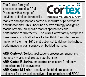 There are many examples of applications that demand the qualities of low cost and efficient performance: connected mobile computers and other portable devices, cellular phones, PDAs, settop box applications, games consoles and autoinfotainment to name just a few.
Consumers don’t just expect their products to do more, they also expect longer battery life for portable products. To achieve all-day use, which is now a minimum requirement, phone, smart phone and PDA manufacturers must deliver extra performance and features more efficiently than before. Consider the smart phone, an application whose performance needs range from an ‘inactive’ state when waiting for a call to very high activity when playing a game. Its system architecture must accommodate both extremes of performance and do it efficiently.
Using a multicore processor architecture is one way to address peak performance demands with a design that is also capable of consuming very low power. Multicore devices deliver highly scalable performance and low power, and so they can offer high levels of design flexibility.
The ARM® Cortexâ„¢-A9 processors are the latest and highest performance ARM processors implementing the full richness of the widely supported ARMv7 architecture. Designed around the most advanced, highefficiency, dynamic length, multi-issue superscalar, out-of-order, speculating 8-stage pipeline, the Cortex- A9 processors deliver unprecedented levels of performance and power efficiency with the functionality required for leading edge products across the broad range of consumer, networking, enterprise and mobile applications.
The Cortex-A9 microarchitecture is delivered within either a scalable multicore processor, the Cortex-A9 MPCore™ multicore processor, or as a more traditional processor, the Cortex-A9 single core processor. Supporting the configuration of 16, 32 or 64KB four way associative L1 caches, the scalable multicore processor and the single processor – two distinct, separate products – provide the broadest flexibility and are each suited to specific applications and markets.
The Cortex-A9 MPCore multicore processor
The Cortex-A9 MPCore multicore processor integrates the proven and highly successful ARM MPCore technology along with further enhancements to simplify and broaden the adoption of multicore solutions. The Cortex- A9 MPCore provides the ability to extend peak performance to unprecedented levels while also supporting design flexibility and new features to further reduce and control the power consumption at the processor and system level.
Targeted implementations of the Cortex-A9 MPCore can also offer mobile devices increased peak performance over today’s solutions by utilizing the design flexibility and advanced power management techniques offered by the ARM MPCore technology to maintain operation within the tight mobile power budgets.
Using the scalable peak performance, this processor is able to exceed the performance of today’s comparable highperformance embedded devices and brings a consistent software investment over an extended breadth of markets.
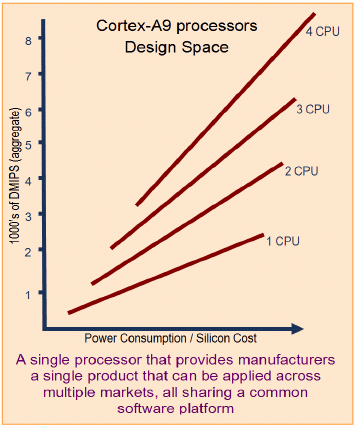
The Cortex-A9 single core processor
The Cortex-A9 processor provides unprecedented levels of performance and power efficiency making it an ideal solution for any design requiring high performance in a low-power, cost sensitive, single processorbased device. Using a convenient synthesizable flow and IP deliverables, the Cortex-A9 processor provides an ideal upgrade path for existing ARM11â„¢ processor-class designs that require higher performance and increased levels of power efficiency within a similar silicon cost and power budget while maintaining a compatible software environment.
The Cortex-A9 single core processor provides dual low-latency Harvard 64-bit AMBA® 3 AXIâ„¢ master interfaces for independent instruction and data transactions and are capable of sustaining four double word writes every five processor cycles when copying data across a cached region of memory.
Meeting the Requirements of Multiple Markets
The Cortex-A9 processors provide a scalable solution across a wide range of market applications from mobile handsets through to high-performance consumer and enterprise products by sharing the common requirements of:
- Increased power efficiency with higher performance for lower power consumption;
- Increased peak performance for most demanding applications;
- Ability to share software and tool investments across multiple devices;
Both Cortex-A9 processors are fully application compatible and can enhance application specific performance by utilizing either the Cortex-A9 NEONâ„¢ Media Processing Engine (MPE) or Floating-Point Unit (FPU), to further extend the range of market applications addressed by these processors.
The design configuration of each implementation then provides the flexibility to tailor the implementation to the application and market-specific characteristics.
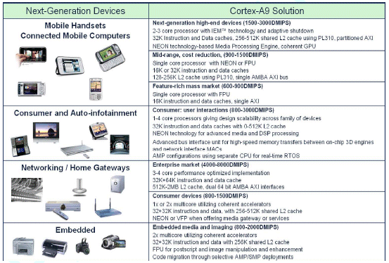
Table 1. Cortex-A9 processor example application profiles
Application Specific Optimization
Both the Cortex-A9 and the Cortex-A9 MPCore application-class processors are supported by a rich set of features and ARMv7 architectural functionality so as to deliver a high-performance and low-power solution across both application specific and general purpose designs.
| Feature | Benefit |
| High-Efficiency Superscalar Pipeline | Industry leading performance with over 2.0 DMIPS/MHz for unprecedented peak performance while also maintaining low power for extended battery life and lower cost packaging and operation |
| NEON Media Processing Engine | Accelerating media and signal processing functions for increased application specific performance with the convenience of consolidated application software development and support |
| Floating-Point Unit | Provides significant acceleration for both single and double precision scalar Floating-Point operations. Double the performance of previous ARM FPU, this unit provides industry leading image processing, graphics and scientific computation capabilities |
| Optimized Level 1 Caches | Performance and power optimized L1 caches combine minimal access latency techniques to maximize performance and minimize power consumption. Also providing the option for cache coherence for enhanced inter-processor communication or support of rich SMP capable OS for simplified multicore software development |
| Thumb-2 Technology | Delivers the peak performance of traditional ARM code while also providing up to a 30% reduction in memory required to store instructions |
| TrustZone® Technology | Ensures reliable implementation of security applications ranging from digital rights management to electronic payment. Broad support from technology and industry Partners |
| Jazelle® RCT and DBX Technology | Provides up to 3x reduction on code size for Just-in-time (JIT) and ahead-of-time compilation of bytecode languages while also supporting direct byte code execution of Java instructions for acceleration in traditional virtual machines |
| L2 Cache Controller | Providing low latency and high bandwidth access to up to 2 MB of cached memory in high frequency designs, or design needing to reduce the power consumption associated with off chip memory access |
| Program Trace Macrocell and CoreSightâ„¢ Design Kit | Together these components provide the software developer with the ability to non-obtrusively trace the execution history of multiple processors and either store this, along with time stamped correlation, into an on-chip buffer, or off chip through a standard trace interface so as to have improved visibility during development and debug |
Table 2. Cortex-A9 processor features
Advanced Microarchitecture
The Cortex-A9 microarchitecture has been designed to maximize processing efficiency within the price sensitivities of embedded devices on silicon cost while trading against the inefficiencies associated with an excessively high frequency design. The result is a processor design that, through synthesis techniques, can deliver devices capable of over 1GHz clock frequency and provide the high levels of power efficiency required for extended battery powered operation.
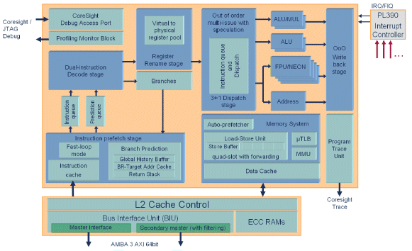
Fig. 1 Cortex-A9 microarchitecture structure and the single core interfaces.
Pipeline description
- Advanced processing of instruction fetch and branch prediction - unblocks branch resolution from potential memory latency-induced instruction stalls.
- Up to four instruction cache line prefetch-pending - further reduces the impact of memory latency so as to maintain instruction delivery.
- Between two and four instructions per cycle forwarded continuously into instruction decode - ensures efficient superscalar pipeline utilization.
- Fast-loop mode - provides low power operation while executing small loops.
- Superscalar decoder - capable of decoding two full instructions per cycle.
- Speculative execution of instructions - enabled by dynamic renaming of physical registers into an available pool of virtual registers.
- Increased pipeline utilization - removing data dependencies between adjacent instructions and reducing interrupt latency.
- Virtual renaming of registers - accelerating code through an effective hardware based unrolling of loops without the additional costs in code size and power consumption.
- Any of the four subsequent pipelines can select instructions from the issue queue - providing out of order dispatch further increasing pipeline utilization independent of developer or compiler instruction scheduling. Ensures maximum performance from code optimized for previous generation of processors and maintains existing software investments.
- Concurrent execution across full dual arithmetic pipelines, load-store or compute engine, plus resolution of any branch each cycle.
- Dependent load-store instructions can be forwarded for resolution within the memory system - further reduces pipeline stalls and significantly accelerating the execution of high level code accessing complex data structures or invoking C++ functions.
- Support for four data cache line fill requests - further reduces stalls due to memory latency with either automatic or user driven prefetching to ensure the availability of critical data.
- Out of order write back of instructions - enables the pipeline resources to be released independent of the order in which the system provides the required data.
The Cortex-A9 MPCore Technology
The Cortex-A9 MPCore multicore processor provides a designconfigurable processor supporting between 1 and 4 CPU in an integrated cache coherent manner. Each processor may be independently configured for their cache sizes and whether the FPU, MPE or PTM interface will be supported. In addition, the processor in any configuration may expose the Accelerator Coherence Port (ACP) permitting other non-cached systemmastering peripherals and accelerators such as a DMA engine or cryptographic accelerator core to be cache coherent with the L1 processor caches. Also integrated is a GIC architecture compliant integrated interrupt and communication system with private peripherals for increased performance and software portability and may be configured to support between 0 (legacy bypass mode) or 224 independent interrupt sources. The processor can support either a single or dual 64-bit AMBA® 3 AXIâ„¢ interconnect interface. The Cortex-A9 MPCore multicore processor includes an enhanced version of the silicon-proven ARM MPCore technology for scalable multicore processing.
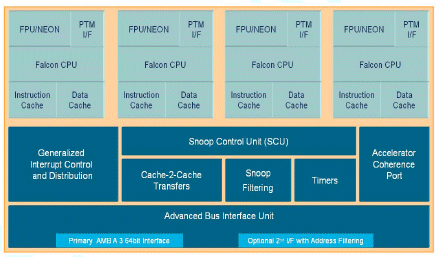
Fig 2. Cortex-A9 multicore processor
Snoop Control Unit
The SCU is the central intelligence in the ARM’s multicore technology and is responsible for managing the interconnect, arbitration, communication, cache-2-cache and system memory transfers, cache coherence and other multicore capabilities for all MPCore technology enabled processors.
The Cortex-A9 MPCore processor for the first time also exposes these capabilities to other system accelerators and non-cached DMA driven mastering peripherals so as to increase the performance and reduce the system wide power consumption by sharing access to the processor’s cache hierarchy. This system coherence also reduces the software complexity involved in otherwise maintaining software coherence within each OS driver.
Accelerator Coherence Port
This AMBA 3 AXI compatible slave interface on the SCU provides an interconnect point for a range of system masters that for overall system performance, power consumption or reasons of software simplification are better interfaced directly with the Cortex-A9 MPCore processor. This interface acts as a standard AMBA 3 AXI slave, and supports all standard read and write transactions without any additional coherence requirements placed on attached components.
However, any read transactions to a coherent region of memory will interact with the SCU to test whether the required information is already stored within the processor L1 caches. If it is, it is returned directly to the requesting component. If it missed in the L1 cache, then there is also the opportunity to hit in L2 cache before finally being forwarded to the main memory. Write transactions to any coherent memory region, the SCU will enforce coherence before the write is forwarded to the memory system. The transaction may also optionally allocate into the L2 cache hence removing the power and performance impact of writing directly through to the off chip memory.
Generic Interrupt Controller
Implementing the recently standardized and architected interrupt controller, the GIC provides a rich and flexible approach to inter-processor communication and the routing and prioritization of system interrupts. Supporting up to 224 independent interrupts, under software control, each interrupt can be distributed across CPU, hardware prioritized, and routed between the operating system and TrustZone software management layer. This routing flexibility and the support for virtualization of interrupts into the operating system, provides one of the key features required to enhance the capabilities of a solution utilizing a paravirtualization manager.
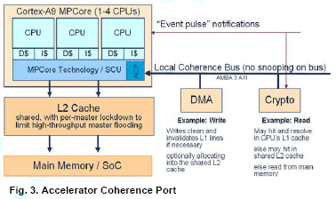
Advanced Bus Interface Unit
Enhancing the interface between the processor and system interconnect, the Cortex-A9 MPCore processor provides advanced features to maximize system performance and offers additional flexibility for various System on Chip design philosophies.
Supporting the design configuration of either a single or dual 64-bit AMBA 3 AXI master interface, the processor can provide, at CPU speed, full load balancing of transactions capable of exceeding 12GB/s into the system interconnect. Alternatively, the second interface may define a transaction filter to a subset of the global address space so presenting the system design with the flexibility to partition the address space immediately within the processor fabric.
Each interface may also offer different CPU to bus frequency ratios, including synchronous half clock ratios for increased design flexibility and improved system bandwidth for designs considering DVFS or high speed on chip memories. Full ARM Intelligent Energy Management (IEM) capabilities can also be supported.
Application Specific Compute Engine Acceleration
In addition to the optimized standard architectural features, both the Cortex-A9 and the Cortex-A9 MPCore processor can be augmented with either of the following architected features:
| Cortex-A9 Floating-Point Unit (FPU): When implemented along with either of the Cortex-A9 processors, the FPU provides high-performance single, and double precision Floating-Point instructions compatible with the ARM VFPv3 architecture that is software compatible with previous generations of ARM Floating- Point coprocessor. Supporting full IEEE- 754 compliant Floating-Point, operating for the first time at the same speed as previous “run-fast†modes, also now operating with no trapped exceptions simplifying software and further accelerating the performance of Floating-Point code. Additional instructions for 16-bit Floating- Point data type conversions have also been added enhancing the interaction with embedded 3D processors such as the ARM Mali™ graphics processors. Providing an average of more than double the Floating-Point performance of previous generation ARM Floating-Point coprocessors, a Cortex-A9 FPU is capable of significantly enhancing solutions with rich graphics, 3D, imaging and scientific computation. | Cortex-A9 NEON Media Processing Engine (MPE): The Cortex-A9 MPE can be used with either of the Cortex-A9 processors and provides an engine that offers both the performance and functionality of the Cortex-A9 Floating-Point Unit plus an implementation of the ARM NEON Advanced SIMD instruction set that was first introduced with the ARM Cortex-A8 processor for further acceleration of media and signal processing functions. The MPE extends the Cortex-A9 processor’s floating-point unit (FPU) to provide a quad-MAC and additional 64-bit and 128-bit register set supporting a rich set of SIMD operations over 8, 16 and 32-bit integer and 32bit Floating-Point data quantities every cycle. Further enhancing the SIMD capability, the MPE also support fused data types to remove packing/unpacking overheads and structured load/store capabilities to eliminate shuffling data between algorithm-format to machine-formats. Utilizing the MPE also enlarges the register file available to FPU and increases the design to support 32 double-precision registers, while retaining the Cortex-A9 processor’s 32/64-bit scalar floating-point and core integer performance. |
Advanced L2 Cache Controller:
The ARM L2 cache controller (PrimeCell® PL310) was designed alongside the Cortex-A9 processors to provide an optimized L2 cache controller that can match the performance and throughput capability of the Cortex-A9 processor.
The PL310 is capable of supporting up to 8 outstanding AXI transactions on each interface, with per-master per-way lockdown to allow managed-sharing between multiple CPU or components using the Accelerator Coherence Port effectively using the PL310 as a buffer between accelerators and the processors therefore increasing system performance and lowering associated power consumption.
The PL310 also includes capabilities of the Cortex-A9 Advanced Bus Interface Unit and therefore also provides support for synchronous ½ clock ratios to reduce latencies on high speed processor designs, and the ability to address-filter second master AXI interfaces for split-domain, split-frequency designs and fast access to on-chip scratch memories.
Supporting up to 2 MB, with between four and sixteen-way associative L2 cache, the PL310 supports the optional integration with both parity and ECC supporting RAM and is capable of operating at the same frequency as the processor. Advanced lock-down techniques also provide mechanisms to use the cache memory as a transfer RAM between coherent accelerators and the processors.
Cortex-A9 Program Trace Macrocell (PTM):
The Cortex-A9 PTM provides ARM CoreSight technology compatible program-flow trace capabilities for either of the Cortex-A9 processors and provides full visibility into the processor’s actual instruction flow. The Cortex-A9 PTM includes visibility over all code branches and program flow changes with cycle counting enabling profiling analysis.
Also available is the Cortex-A9 CoreSight Design Kit which enables correlation of trace streams from multiple processors and includes all of the CoreSight components required to trace and debug a Cortex-A9 MPCore multiprocessor design.
Syntheses Flexibility and Reference Methodologies
Utilizing the full flexibility of a syntheses design flow, the Cortex-A9 processor deliverables are capable of being targeted to any foundry process and geometry. Through continued collaboration with leading EDA companies there will also be available Implementation Reference Methodologies (iRMs) that enable Cortex- A9 processor licensees to customize, implement, verify and characterize the processors across their chosen process technologies. These reference methodologies provide a predictable route to silicon, and a basis for custom methodology development, using both logical and physical synthesis techniques. In additional the iRMs can contain ARM Artisan® front-end library views, and pre-compiled RAMs to enhance the ability of the iRMs to deliver processor implementation flows and provides a far more complete reference solution than previously offered.
Tools & Ecosystem
Tools Support
All ARM processors are supported by the ARM RealView® portfolio of development tools, as well as a wide range of third party tools, operating system and EDA vendors.
ARM RealView tools are unique in their ability to provide solutions that span the complete development process from concept to final product deployment. Each member of the RealView portfolio has been developed closely alongside the ARM hardware and software IP, ensuring that it maximizes the IP's performance. No other supplier can offer this unique end-to-end toolchain support for ARM IP, from system and processor design through software development.
Working with ARM RealView tools provides an extensive and cohesive product range that empowers architects and developers alike to confidently deliver optimal products into the marketplace faster than ever before.
Third party support
The ARM Connected Community is the industry’s largest network of leading silicon, systems, design support, software and training providers enabling system designers to access a huge range of ARM technology and optimized IP to provide a complete solution, from design to manufacture and end use, for products based on the ARM architecture. For more information, please visit http://www.arm.com/community.
Physical IP
ARM’s Artisan Physical IP products are designed to achieve the best combination of performance, density, power and yield for a given manufacturing process. The products are available for 45- through 250- nanometer processes and delivered with an extensive set of views and models supporting industry leading EDA tools. ARM Artisan IP platforms and product portfolios offer a wide range of choices to meet systemon- chip (SoC) designers’ nanometer requirements.
AMBA
The AMBA interconnect protocol forms the basis of the de facto industry-standard on-chip interconnect specification that serves as a framework for SoC designs, effectively providing the “digital glue†that binds IP components together. It is also the backbone of the ARM design reuse strategy. Through consultation with the wider SoC community, ARM strives to achieve the most technologically advanced, supportable, royalty-free interconnect specification in the industry. The current PrimeCell portfolio of peripheral IP supports the AMBA 2 and 3 release of the protocol that defines the AMBA AXI™, AHB™, AHB-Lite, APB, and ATB specifications. For further information on the AMBA protocol, please see http://www.amba.com.
Summary
The Cortex-A9 and Cortex-A9 MPCore are two new ARM processors designed to address the requirements for both single and multiple processor designs. The common microarchitecture incorporates features that provide enhanced architectural functionality, performance and power efficiency across not only the processor core, but the entire SoC.
The single core processor offers higher performance and increased power efficiency for existing ARM11 class devices enabling enhanced functionality and lower power consumption for extended battery life in mobile designs. The implementation characteristics also provide full architectural software compatibility to enable cost-reduction at Cortex-A8 class performance to extend the market reach of the associated software investments.
The MPCore implementation of the processor offers advanced power management features to further lower power consumption and exceed the power requirements across an increasing number of markets and applications. The Cortex-A9 MPCore also delivers unprecedented levels of scalable performance opening markets previously unable to enjoy the power efficiency inherent in the design of an ARM processor. The complete range of companion technology was specifically designed to integrate with both the Cortex- A9 processors to boost performance further as required in specific applications and markets, especially within wireless, entertainment, imaging and other high-end multimedia applications.
ARM Cortex-A9 MPCoreâ„¢ processor: A multicore processor that delivers the next generation of the ARM MPCore technology for increased performance scalability and increased control over power consumption. Ideal for high-performance mobile handsets, networking and auto-infotainment devices.
ARM Cortex-A9 processor: A traditional single core processor for simplified design migration in high-performance, cost-sensitive markets such as mobile handsets and other embedded devices, reducing time-to-market and fully maintaining existing software investments.
THIS WHITEPAPER CONTAINS PRELIMINARY INFORMATION AND DETAILS MAY CHANGE BEFORE ACTUAL PRODUCT RELEASE
