By Pankaj Singh, Texas Instruments India (P) Ltd
Abstract :
In today’s fast growing Systems-on-Chip (SoC), incomplete or ineffective DFT (Design For Test) support/deliverable due to poor specification or tool limitation/flow gap can quickly become the critical path in meeting market windows and delivering products within cost restrictions.
In spite of improvement in design flow/ methodologies we continue to see issues during silicon validation due to incomplete test deliverables, gaps in flow or difference in simulation and tester environment. Even after completing the QC checks often the Quality of test pattern handoff depends on the experience of DFT engineer and requires manual correction/effort before handoff to PE (Product Engineering) team. In past Joel Graber has presented his work well on VLCT (Very Low Cost Tester) limitation, mismatch between simulation and tester [1]. However there is no automated utility to identify and fix these issues on test patterns prior to handoff to PE team causing schedule delay.
This paper introduces a unified DFT - PE Methodology, aimed at providing a complete, methodical and fully automated path addressing gaps between DFT and PE team ensuring quick turnaround time in silicon validation. The methodology used in this paper significantly improved the cycle time for silicon validation using low cost tester. The know-how of issues described in this paper has been successful in achieve 93% digital test pattern passing in silicon within a day and 98% digital test pattern pass within a week time frame thereby significantly reducing the silicon validation time.
This paper start with introduction section which describes critical WIMAX (Worldwide Interoperability for Microwave Access) silicon validation issues experienced over last two years and highlights the need for unified methodology to overcome these issues. Summary of silicon validation issues described in this section are based on lessons learned between design team, product engineering team and analog IP team.
The next section provides details on solution offered in this paper. This section describes details on how proposed methodology overcomes limitations mentioned in the introduction section. It lists features, benefits of this utility and depicts the implementation details to the user.
The last section concludes this paper with overall benefits of the proposed methodology and lists limitation/scope for future work.
I. INTRODUCTION
This section starts with summary of all lessons learned/issues categorized on WIMAX project
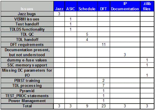
Table1. WIMAX Silicon Validation Issues [2].
Often a cultural gap exists between DFT and product engineering teams due to incomplete understanding of silicon validation (JAZZ flow, IDDQ (Integrated Circuit Quiescent Current) requirements) by DFT engineers and vice versa for PE team causing multiple test pattern handoff and test time/money. What passes in simulation may not necessarily pass in silicon on tester. There have been a series of contributing factors for this oversight:
The DFT Methodology proposed in this paper is defined into three separate sections:
This section depicts the implementation details, highlighting features and benefits.
A. Automated TDL Rules Utility
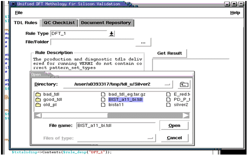
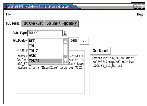
Figure1. Snapshot of TDL Rules.
These rules can be run on individual TDL file/dir
B. QC Checklist/Lessons Learned
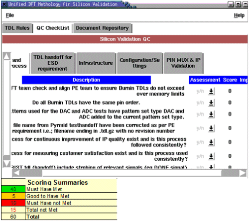
Figure2. Snapshot of QC Checklist
C. Central Document Repository
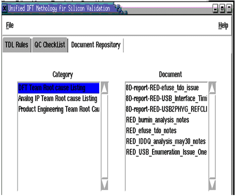
Figure3. Snapshot of Document Repository.
I I I. Conclusions
In this paper presents DFT-PE methodology is presented which minimizes handoff issues between DFT-PE teams and provides workable solution/utility to support early silicon validation:
While the work presented in this paper is focused on WIMAX projects only; most of the rules/score based checklist are generic and can be reused/expanded for include other SoC design projects.
Acknowledgement
This paper would not have been possible without active contributions from Analog IP, Product Engineering and RED DFT team in resolving all open issues in WiMAX SoC : RED; Silicon validation. Special thanks to Rosal Juan in driving effort from TI Management to brainstorm root cause analysis across different groups and also to Vyagrheswarudu Nainala in showing me good/bad TDL scenario/examples which was useful to me in developing Rule based utility.
References
Pankaj Singh completed his bachelors in electronics from REC Bhopal in 1993; Master’s in electrical engineering from USF, Florida in 1997 and an MBA from SMU, Dallas in 2001. In the past he has worked in various design lead roles such as IP development Manager, functional verification Manager. Currently he is engaged with TI India WTBU organization as WIMAX SoC design Manager
B. Appendix
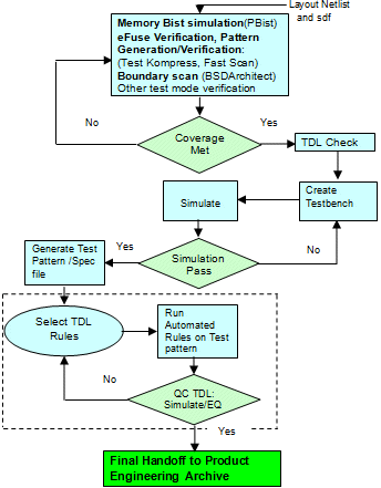
Figure4. Post DFT Verification Flow
Abstract :
In today’s fast growing Systems-on-Chip (SoC), incomplete or ineffective DFT (Design For Test) support/deliverable due to poor specification or tool limitation/flow gap can quickly become the critical path in meeting market windows and delivering products within cost restrictions.
In spite of improvement in design flow/ methodologies we continue to see issues during silicon validation due to incomplete test deliverables, gaps in flow or difference in simulation and tester environment. Even after completing the QC checks often the Quality of test pattern handoff depends on the experience of DFT engineer and requires manual correction/effort before handoff to PE (Product Engineering) team. In past Joel Graber has presented his work well on VLCT (Very Low Cost Tester) limitation, mismatch between simulation and tester [1]. However there is no automated utility to identify and fix these issues on test patterns prior to handoff to PE team causing schedule delay.
This paper introduces a unified DFT - PE Methodology, aimed at providing a complete, methodical and fully automated path addressing gaps between DFT and PE team ensuring quick turnaround time in silicon validation. The methodology used in this paper significantly improved the cycle time for silicon validation using low cost tester. The know-how of issues described in this paper has been successful in achieve 93% digital test pattern passing in silicon within a day and 98% digital test pattern pass within a week time frame thereby significantly reducing the silicon validation time.
This paper start with introduction section which describes critical WIMAX (Worldwide Interoperability for Microwave Access) silicon validation issues experienced over last two years and highlights the need for unified methodology to overcome these issues. Summary of silicon validation issues described in this section are based on lessons learned between design team, product engineering team and analog IP team.
The next section provides details on solution offered in this paper. This section describes details on how proposed methodology overcomes limitations mentioned in the introduction section. It lists features, benefits of this utility and depicts the implementation details to the user.
The last section concludes this paper with overall benefits of the proposed methodology and lists limitation/scope for future work.
I. INTRODUCTION
This section starts with summary of all lessons learned/issues categorized on WIMAX project
- A total of 51 lessons learned were identified.
- Three groups within Wireless own the majority of the issues (Top level design / Analog IP design / PE team)

Table1. WIMAX Silicon Validation Issues [2].
Often a cultural gap exists between DFT and product engineering teams due to incomplete understanding of silicon validation (JAZZ flow, IDDQ (Integrated Circuit Quiescent Current) requirements) by DFT engineers and vice versa for PE team causing multiple test pattern handoff and test time/money. What passes in simulation may not necessarily pass in silicon on tester. There have been a series of contributing factors for this oversight:
- Unwritten rules : There are a lot of “known†rules that are not spelled out anywhere. The discrepancy between simulated TDL(Test Description Language) and TDL run on tester due to flow limitation/issues results in multiple TDL handoff/QC issues:
- PLL(Phase Locked Loop) TDL's for VLCT require two clocks, which is not required on any other tester.
- Pattern set type must be spelled out in order to run VERMI
- BIST(Built-In Self-Test) TDL's require strobing of DONE signal
- Understanding analog IP setting as per configuration settings in valid state/mode .
- PLL shutdown requires BYPASS mode
- Valid mode : Only power on and retention for some subchip/module and no power down mode for IDDQ measurement
- Methodology failures
- Alert for memories used for functional mode, but not reviewed for test mode.
- Assumption that some IP did not change from previous version of the project to new version of the project resulted in incomplete review from IP owner (e.g. missing port definition in one of the analog IP causing metal release)
- Documentation
- Incorrect I/O sheet describing lowest power setting for I/Os: Unnecessary TDL regeneration and debug to achieve quiescent mode power.
- Incomplete integration specification: missing clock usage description for STA(Static Timing Analysis). This caused major problem with functional fail due to incorrect sdf (Standard Delay Format) annotation resulting in interface level timing issue. Two months of engineering team effort was spent by customer, India, US engineering team to debug /validate the issue with multiple FIB’s (Focused Ion Beam) eventually resulting in MLR (Metal Level Revision). Apparently same issue was already found earlier and fixed in previous version/project but was missed in next/new project.
- Incomplete description of shutdown mode in PLL documentation: No description that BYPASS is necessary for shutdown. This resulted in multiple TDL handoff and tester debug time to meet the shutdown power requirement as per specification.
- Improper naming convention for powerdown control in one of the analog IP resulted in incorrect TDL configuration/setting and regeneration/handoff of patterns to PE team.
The DFT Methodology proposed in this paper is defined into three separate sections:
- First section is rule based utility which implements some of these lessons learned ensuring completeness of DFT closure. It minimizes product engineering issues/re-delivery of TDL's due to incomplete QC/handoff of pattern and overcomes existing flow limitation.
- Second section maintains score based checklist (DFT-PE silicon validation checklist not DFTM) based on these lessons learned highlighting gaps in DFT closure for silicon validation. 100% compliance on mandatory listing ensures minimal issues and early silicon bring-up.
- The last section includes library of useful documents (1page summary/8-D report) from real examples/lessons learned to ensure lessons learned are not lost and zero repeat of mistakes.
This section depicts the implementation details, highlighting features and benefits.
A. Automated TDL Rules Utility
- Features:
- Provides set of automated rules implemented from real examples/issues reducing chances of TDL re-delivery.
- Allows the user to select the rules and run it on either individual files or complete directory.
- Provides user with option to view the results and save the final/corrected TDL file.
- Benefits:
- Improves quality of test pattern deliverable and supports early silicon bring up. Minimizes TDL re-delivery by overcoming existing flow limitation and mismatches between VLCT tester and simulation.
- Saves time due to manual effort of correcting individual TDL patterns prior to handoff.
- Less prone to error since the rules are validated and automated as compared to manual update which is dependent on experience of DFT engineer.
- Modular rules structured as functions allowing new rules to be added with ease


Figure1. Snapshot of TDL Rules.
These rules can be run on individual TDL file/dir
B. QC Checklist/Lessons Learned
- Features:
- Includes list of score based checklist incorporated from past lessons learned/8-D reports.
- Allows users with flexibility to define importance (mandatory/optional) for checklist as per project requirement.
- Summarizes overall score, providing useful insight to the user on improvement areas.
- Benefits:
- Ensures past mistakes are not repeated: All lessons learned from past projects are incorporated as part of checklist reducing human error due to change in engineering teams.

Figure2. Snapshot of QC Checklist
C. Central Document Repository
- Features:
- Supports interface to acrobat and html viewer (acroread, html) to load internal 8-D report/1-page issue summary from central repository.
- Categorizes each document for easy listing: DFT, PE, SoC design, IP team.
- Supports easy document update to central repository.
- Benefits:
- Promotes usage of best practices from past lessons learned.
- Provides single access point to useful documents to engineering/management team.

Figure3. Snapshot of Document Repository.
I I I. Conclusions
In this paper presents DFT-PE methodology is presented which minimizes handoff issues between DFT-PE teams and provides workable solution/utility to support early silicon validation:
- Minimizes issues due to mismatch between VLCT and simulation by providing automated/error free rules to correct the TDL pattern post DFT verification for tester.
- Score based methodology to give useful insight on completeness of QC process.
- Central repository with easy access to list of 8-Dreports/issues providing clear understanding of past issues and promoting best practices.
While the work presented in this paper is focused on WIMAX projects only; most of the rules/score based checklist are generic and can be reused/expanded for include other SoC design projects.
Acknowledgement
This paper would not have been possible without active contributions from Analog IP, Product Engineering and RED DFT team in resolving all open issues in WiMAX SoC : RED; Silicon validation. Special thanks to Rosal Juan in driving effort from TI Management to brainstorm root cause analysis across different groups and also to Vyagrheswarudu Nainala in showing me good/bad TDL scenario/examples which was useful to me in developing Rule based utility.
References
[1] Joel G . “Closing the TDL QC Loop on VLCT: Design Simulation of VLCT events†in TI Symposium on Test – 2004
[2] Rosal, J “WIBRO/WIMAX Issues†in TI Wireless Management Review, Dallas May 2007.
[3] Stylianos D, Iraklis D and Thanasis O, “A Unified DFT Verification Methodology.†in IPSoC 2005
[4] Siva Y, “Addressing Post Silicon Validation Challenge: Leverage Validation & Test Synergy†in IEEE International Test Conference Oct 25, 2006
BIOGRAPHYPankaj Singh completed his bachelors in electronics from REC Bhopal in 1993; Master’s in electrical engineering from USF, Florida in 1997 and an MBA from SMU, Dallas in 2001. In the past he has worked in various design lead roles such as IP development Manager, functional verification Manager. Currently he is engaged with TI India WTBU organization as WIMAX SoC design Manager
B. Appendix

Figure4. Post DFT Verification Flow
