Introduction:
Aggressive ground rule changes continue to increase the complexity of semiconductor technology. The requirements for designs, processes, equipment, and facilities all grow in sophistication from generation to generation. These trends have made it increasingly difficult to produce a technology in the development laboratory and transfer it to volume manufacturing in a timely and cost effective manner. The traditional laboratory role of design and process development has expanded to include a parallel responsibility for manufacturability. For many companies, design for manufacture (DFM) has become a critical strategy for survival in an increasingly competitive global marketplace. DFM is a systems approach to improving the competitiveness of a manufacturing enterprise by developing products that are easier, faster, and less expensive to make, while maintaining required standards of functionality, quality, and marketability. Design for manufacturability (DFM) and early manufacturing involvement (EMI) concepts are now major components of the development effort designed to maintain and enhance the rate of technology advancement and significantly improve the development-to-manufacturing transition. Design-for-manufacturability philosophy and practices are used in many companies because it is recognized that 70% to 90% of overall product cost is determined before a design is ever released into manufacturing. The semiconductor industry continues to grow in both complexity and competitiveness.
This paper describes the causes of yield drop out in deep submicron technologies and methods to improve yield at design and manufacturing stage of IC development cycle.
Problem Statement
The layout development is most critical in integrated circuits (IC's) design because of cost, since it involves expensive tools and a large amount of human intervention, and also because of the consequences for production cost. As the device size is shrinking, the landscape of technology developments has become very different from the past. The problems, which were supposed to be secondary can cause of yield drop out in submicron technologies. The variability becomes a critical issue not only for performance, but also for yield dropout.
Yield dropout due to given below defects.
1. Random Defects: Due to form of impurities in the silicon itself, or the introduction of a dust particle that lands on the wafer during processing. These defects can cause a metal open or shorts. As feature sizes continue to shrink, random defects have not decreased accordingly making advanced IC’s even more susceptible to this type of defect.
2. Systematic Defects: Again systematic defects are more prominent contributor in yield loss in deep submicron process technologies. Systematic defects are related to process technology due to limitation of lithography process which increased the variation in desired and printed patterns. Another aspects of process related problem is planarity issues make layer density requirements necessary because areas with a low density of a particular layer can cause upper layers to sag, resulting in discontinuous planarity across the chip.
3. Parametric Defects: In deep submicron technology parametric defects is most critical for us. Parametric defects come into the picture due to improper modeling of interconnects parasitic. As a result manufactured device does not match the expected result from design simulation and does not meet the design specification.
Design for manufacturability (DFM) is process to overcome these defects of yield drop out. The DFM will not be done without collaborations between various technology parties, such as process, design, mask, EDA, and so on. The DFM will give us a big challenge and opportunity in nanometer era.
DESIGN FOR MANUFACTURABILITY:
Design for Manufacturability is the proactive process which ensures the quality, reliability, cost effective and time to market.
DFM consist a set of different methodologies trying to enforce some soft (recommended/Mandatory) design rules regarding the shapes and polygons of the physical layout which improve the yield.
Given a fixed amount of available space in a given layout area, there are potentially multiple yield enhancing changes that can be made.
There are some DFM guidelines which we can take into account during layout.
- Antenna effect guidelines
Configuration: Identify poly gates connected to large areas of metals.
Action: Reduce the ratio surface of metal/surface poly gate or use free wheel diode.
Reasons for this action: During process, the wafers are submitted to plasma environments. Because of metallization, electrons are collected. Because of mirror effects charges accumulate at the gate oxide. An electric field is created and can cause oxide breakdown.
- Minimum Area of physical layers
Configuration: Identify very small rectangle of a given layer (typically shape at the min area size like diffusion)
Action: Try not to draw shapes at min area when free space is available around.
Reasons for this action: Process window can allow shapes to be at min area, but if these shapes are numerous, risk is higher that some of them are not resolved: for instance, in case of implant, that would lead to missing implant. Typical case: Pwell and Nwell Straps (Ties).
- Density Gradient
Configuration: Identify high density areas next to low density areas.
Action: Try to balance shapes to reach homogeneous density and add dummy patterns.
Reasons for this action: Density of some layers (specifically those treated by Chemical & Mechanical Polishing (CMP) like diffusion, poly and metals) has a big impact on the manufacturing of the given pattern. Impact is both on CMP processing and PHOTO processing. Too high gradient can lead to shorts or opens.
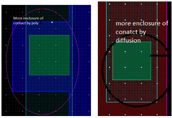
- Contact Enclosure by Diffusion/poly silicon

Configuration: Identify min enclosure of contacts by diffusion.
Action: Try to extend the enclosure of contact by diffusion area when possible.
Reasons for this action: Overlay could make that one contact falls on the border of the diffusion area, thus generating a junction leakage.
Caution: Proportions of the dimensions of this transistor have not been kept, for a better visibility of the example. Take care of resulting increase of drain capacitance.
- Metal extension of Via/contact at Line Ends

Configuration: Identify Via transitions at line ends.
Action: Try to extend the overlap of metals at line ends.
Reasons for this action: Process window issues might lead to resistive or even open vias. Extending metals overlap ensures a better transition.
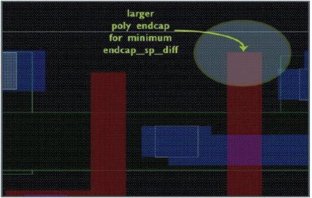
- Gate Extension on Diffusion (End Cap)

Configuration: Identify poly gate of transistor at min from diffusion.
Action: Try to extend the poly end cap wherever it is not too close to other structures
Reasons for this action: Silicon implementation of this configuration could lead to leakage current between drain and source of the given transistor. Do not draw at min if space is available.
- Contact/Via Redundancy
Configuration: Identify single contact specifically for critical transistor in repetitive cell.
Action: Try to double contact and extend poly and metal1 without impacting too much on poly & metal1 critical area.
Reasons for this action: Single contacts can be more sensitive to defect and resistivity spread especially in case of L transition. Salicide discontinuity risk is also present. Inserting a new contact reduces probability to have a too resistive (or even open) transition, and reduces electro-migration effect.
- Metal to Metal spacing
Configuration: Identify wires at min spacing with free space around
Action: Do not keep min spacing. Try to spread these wires and if not possible decrease width/space ratio.
Reasons for this action: Long wires at min spacing increase probability to have shorts due to particles
- Via/contact to Via/contact spacing
Configuration: Identify large Via to Via spacing.
Action: Decrease Via to Via spacing by adding dummy vias.
Reasons for this action: Lone Vias or edge Vias tend to be gathering points of Low K outgasing. This results in resist poisoning and poor Vias lithography and etching => Via Opens
Note: Dummy vias must be added above metal lines or dummies.
Regular layouts
There are some DFM guidelines which we can take into account at SOC level.
1. Filler cell (consisting regular Diffusion and Poly silicon structures) insertion and shielding
Issue Addressed: PO/OD non uniformity
Benefit: Higher parametric yield.
2. Via optimization
Issue Addressed: open Via’s, systematic via opening issue
Benefit: Higher yield after manufacturing and qualification.
3. Wire Spreading
Issue Addressed: wire shorts and opening due to defectivity.
Benefit: Higher yield, decrease cross talk.
4. Power/ground-connected fill
Issue Addressed: Density gradients, Large IR drop, Layout becomes regular
Benefit: Robustness to IR drop
5. Litho hotspot detection and repair
Issue Addressed: Lithography hotspots
Benefit: Higher yield
6. Dummy Metal/Via/FEOL
Issue Addressed: Large density gradients
Benefit: Higher yield
7. CMP hotspot detection
Issue Addressed: CMP hotspots
Benefit: Higher yield
References: Impact of DFM and RET on Standard-Cell Design Methodology by Paul de Dood
Authors:
Rahul Saxena, Deepak Sharma, Sachin Kalra, Azeem Hasan, Vikas Garg
Freescale Semiconductors Ltd
