By Andrew Cole, Silicon Creations
Abstract:
Fractional-N PLLs are a useful class of PLLs and not well understood. This paper explains in simple terms how these differ from a regular integer PLL. Common applications are listed along with a brief description of the key performance parameter – jitter.
With a combination of slow analog circuits and fast digital logic N PLLs cannot be properly simulated with traditional SPICE. AFS from Berkeley Design Automation performs these simulations accurately.
Simulation results are compared to measurements of a Fractional-N PLL in TSMC 28nm HPM CMOS. The correlation is excellent so that reliable jitter/area/power tradeoffs can be made.
The authors experience AFS runtimes up to 20 times shorter than traditional SPICE so that these simulations can be completed without impacting tight schedules.
Fractional-N PLLs - Construction and Applications
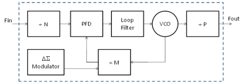
A simplified block diagram of a Fractional PLL is shown in Figure 1. Excluding the block marked Δ Σ (Delta-Sigma) Modulator, this PLL is same as a conventional PLL. A Phase-Frequency Detector (PFD, including a charge pump) compares a divided version of the VCO clock with a divided version of the PLL input. The PFD outputs are filtered by the loop filter and adjust the VCO frequency up or down until the two PFD inputs are in phase with each other. At this point the PLL is locked and the two PFD input frequencies are exactly the same (on average). Post dividers (÷ P) are often used to divide a higher VCO frequency down to a useful frequency.

Figure 1 – Fractional-N PLL Block Diagram
This PLL arrangement is known as an integer PLL and allows a frequency of FIN*M/(N*P) to be generated. The resolution in output frequency is FIN/(N*P). By making these dividers larger, finer resolution can be obtained. However, this improvement comes at a cost of power (as the VCO must run faster) and compromised PLL loop stability.
The Δ Σ modulator varies the feedback divider value over time such that the average of the values is a desired fractional value. For example, a fractional divide value of 10.25 can be achieved by the following set of divide values: 10, 10, 10, 11, 10, 10, 10, 11, and so on. Using this method the PLL output can be adjusted in much smaller increments while keeping the VCO frequency (and power) relatively low.
This sequence has a drawback. The pattern repeats at a rate of FPFD/4 (a quarter of the frequency at the input to the PDF). Unless the loop filter bandwidth is very low this can cause jitter in the VCO output frequency. The following sequence of divide values: 10, 12, 8, 11, 8, 12, 10, 11, … also has an average of 10.25. However, the excursions occur more rapidly which places lower demands on the loop filter saving die area. This more complicated sequence might be generated by a “2nd order†modulator choosing between 5 values.
The Δ Σ modulator is a special class of modulator preferred for this application because it varies the divider values in a pseudo-random way so that the frequency tones generated in the PLL output (the “fractional noiseâ€) resemble random noise.
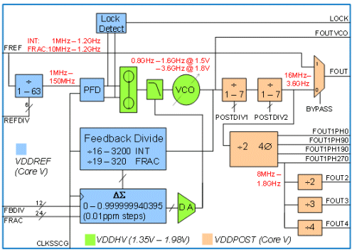
Nevertheless, when extremely small increments in output frequency are desired the sequences will be long and fractional noise can appear. The Silicon Creations Fractional-N PLL (block diagram shown in Figure 2) suppresses this noise with the addition a feed-forward compensator that feeds directly into the loop filter, and is able to achieve jitter in Fractional mode very close to that achieved in integer mode. Long term jitter as small as 2ps RMS has been measured in fractional mode.
This Fractional-N PLL is clearly much more versatile than an integer PLL. With modern CMOS processes the logic required for the Δ Σ modulator occupies only a modest amount of silicon and provides many benefits. The TSMC 28nm HPM CMOS PLL in Figure 2 is only 0.06mm2. A 24-bit modulator allows the output frequency to be adjusted in steps of at most 1/(M*224) = 0.003ppm when M = 19 – practically continuous adjustment.
Fractional-N PLLs are used for many applications falling into two main groups:
- Providing clock signals for system logic
- Timing for Data Converters and RF systems
When generating clock signals for system logic the Fractional-N PLL provides almost complete freedom in choosing the clock reference frequency. This increases the market lifetime of chips and allows manufacturers to change crystals after starting production. If the modulator target is changed over time the PLL output can generate a clock with a known spectrum. In this way an accurate Spread Spectrum Clock Generator (SSCG) can be created.
The high-speed logic designer needs to know the shortest clock period the logic will encounter. Thus the PLL Period Jitter (PJ, also known as short term jitter) must be known in order for the circuit to have sufficient timing margin.
System designers using the Silicon Creations Fractional-N PLL to clock data Converters and RF systems appreciate the extremely fine adjustments possible in frequency without having to compromise in jitter. For these systems the deviation of the PLL output edges from their ideal position, the PLL Long Term Jitter (LTJ) is important. For example, when the PLL output clock is used to determine the sampling moment for an analog input signal the LTJ determines the system distortion, or analog noise floor.
In most chips the PLL is critical and system performance usually depends on the PLL meeting jitter specifications. To stay competitive, chip makers rely upon their PLL IP suppliers making reliable power/area/performance tradeoffs that are met with first silicon. A trustworthy simulation environment is essential.
Fractional-N PLLs – Simulation and Challenges
PLLs present a number of challenges to the circuit simulator.
The first is simulation time. The Loop Filter will commonly have a bandwidth in the range of 10kHz to 1MHz. When simulating the PLL in transient mode we must simulate for a time exceeding many time constants of this loop filter in order for the PLL to settle. But modern PLLs also include a large amount of high-speed digital logic. In order for the TSMC 28nm HPM PLL shown in Figure 2 to recover from any condition this logic must operate beyond the highest frequency the VCO can generate in a fault condition. This means the logic includes custom gates with edge rates compatible with operation at close to 10GHz. These edges force hundreds of transient timesteps per 10GHz period leading to very long runtimes.

Figure 2 – Silicon Creations TSMC 28nm HPM Fractional-N PLL
The second challenge, exacerbating this is dynamic range or accuracy. Default SPICE RELTOL is 0.1%. But node voltages will have numerical noise on the same order and significantly impact the jitter we are trying to measure. In order for the PLL to be accurately simulated the simulator must iterate until the voltages are computed to a level of accuracy matching the desired dynamic range. The Figure 2 PLL easily achieves effective dynamic range exceeding 100dB, and when the VCO is replaced by a higher quality LC oscillator it can comfortably exceed 120dB.
Simulating this PLL from power-on to lock in conventional SPICE can take many weeks which presents the project planner with an unpleasant choice – delay the project or proceed at risk.
Silicon Creations uses Analog FastSPICETM (AFS) from Berkeley Design Automation (BDA) to avoid this choice. The simulation time speed-up offered by AFS allows us to deliver our PLLs without delays, and with the confidence provided by a complete PLL transient simulation.
In all PLL applications jitter is a key performance parameter and can be simulated in two ways with AFS.
- Periodic Noise Analysis for periodic blocks.
- Transient Noise Analysis for all circuits, including the closed-loop PLL.
In a well-designed PLL the VCO is the dominant noise source. Periodic Noise Analysis which runs very quickly can be used to verify the VCO design over a large number of PVT corners and with Monte Carlo variations in devices.
To be certain the PLL is operating correctly we need to include the entire circuit, with parasitic elements extracted from the layout and run a transient simulation. AFS can run a Transient Noise simulation where random thermal and flicker noise is added based on instantaneous bias for each device at each timestep. AFS can do this while keeping the simulation time below 2X the time taken for a transient simulation without device noise.
This modest overhead was a factor for Silicon Creations in choosing AFS because other simulators offering Transient Noise cut corners by not calculating random device noise at every step. This can reduce the accuracy of the simulation.
When a simulation tool offers two independent ways of generating the same information it is key that they provide the same results. The simulation results and measurements shown further in this paper show that the results of Periodic Noise Analysis and of Transient Noise Analysis match the silicon measurements, and consequently each other.
Silicon Creations’ results are not unique. BDA’s Analog FastSPICETM is published as a TSMC Analog Reference Design Flow since 2010 meaning BDA has shown this correlation with multiple analog and mixed-signal circuits using TSMC process technologies.
Comparing Simulations to Silicon
Silicon Creations has compared the results of silicon measurements of its TSMC 28nm HPM Fractional-N PLL to the predictions made by AFS. We also compared simulation runtimes to multiple SPICE simulators. This section briefly describes these simulations and the results.
Periodic Noise Analysis runs quickly and we compared results at a number of PVT conditions and VCO operating frequencies. Figure 3 shows two results typical of the comparisons with the silicon measurements (using a spectrum analyzer) overlying the same graphs. For the measurements the PFD frequency was set to a low value. The loop filter bandwidth in this PLL scales automatically with FPFD making the design very robust. This allowed us to compare the VCO noise prediction to measurements over a wide range by using a low FPFD. The simulated VCO noise above the loop bandwidth tracks the PLL measurements within a couple of dB. This is an excellent correlation and provides confidence the VCO is indeed well designed and will perform will over process corners we have not seen silicon for.

Figure 3 – VCO Phase Noise Simulation vs. Measurements – 0.9GHz and 1.5GHz Hz, 125°C
These plots are “phase noise†plots and show the amount of noise in the PLL output phase relative to the output signal level at various frequency offsets from the output signal frequency. The units of the vertical axis are dBc/Hz. Integrated over the entire frequency range these plots provide the total RMS jitter of the signal being measured. The amount of jitter missed by starting at 1kHz is tiny compared to that seen above 1kHz. In the upper part of the figure the noise falls off at 40dB/decade meaning the noise frequencies to the right of these figures also contribute very little to the jitter.
Presenting the PLL noise in this way is important for systems that are able to track noise at low frequencies and are insensitive to (a small amount of) noise at very high frequencies. Serializer-Deserializer circuits and many RF systems fall into this category and the designers of these systems will observe the shape of the phase noise plots and the level of phase noise to gage the quality of the clock signal within the frequency range their system is most sensitive.
To gain a complete picture of the noise we need to run a Transient Noise Analysis of the closed loop PLL with all circuits operating. This includes the jitter generated by the fractional modulator and the impact of the feed-forward compensation circuit. This PLL’s 18,100 MOS transistors provide an extracted circuit with 108,000 circuit elements – a tough circuit for any simulator. With the complex 28nm models from TSMC this simulation takes about four days running with four parallel CPUs (3.4 GHz Intel i7-2600). The transient time simulated was 100 times the period of the period of the lowest noise frequency analyzed (BDA suggests at least 40 times).
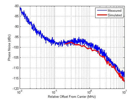
Figure 4 shows an overlay of the post-processed closed-loop PLL transient noise simulation result with the measured Fractional-N PLL phase noise. Over most of the range the correlation between measurement and the prediction is excellent.

Figure 4 – PLL Transient Noise Simulation vs. Measurement
The total integrated jitter of this PLL measured from 10kHz to 100MHz is 1.8ps. Integrating from 10kHz to 10MHz provides a result of 1.6ps, showing that little accuracy is lost by terminating the measurement at 10MHz. The deviation between the measurement and the simulation close to the loop bandwidth integrates to 0.2ps – a very small difference in the end result.
Potential causes for the difference between the measurement and the simulation include power supply noise from the voltage regulator on our test PCB, a difference in measurement and simulation temperature.
The accuracy of this correlation has been demonstrated multiple times and the results correlate well with the Periodic Noise results. This gives us great confidence in the results from AFS and provides our customers with assurance that the power, area and performance tradeoffs we have performed to optimize the PLLs we deliver to them will be seen in their products. The runtime of this simulation makes it practical as a sign-off simulation when the jitter is critical.
Traditional SPICE simulators do not offer feasible Transient Noise capabilities so we cannot compare simulation runtime with SPICE.
For many system designers the time the PLL takes to lock from startup is important. With its 108,000 extracted circuit elements this PLL a regular Transient simulation is very challenging for SPICE. The node voltage accuracy mentioned above is important as small errors can accumulate resulting in wildly inaccurate predictions of locking time.
Figure 5 shows the loop filter voltage of this PLL in two operating modes as the PLL moves from power on to locking. In integer mode (with the Δ Σ Modulator turned off) the lock time simulated by AFS is 15.6µs, very close to the measured 15.8µs. The predicted lock time in Fractional mode is similarly accurate.

Figure 5 – PLL Transient Noise Simulation vs. Measurement
With traditional SPICE this simulation takes roughly three weeks. With AFS we completed this simulation in 30 hrs, a speedup of 18×. Consequently we are able to include LOCK simulations as a sign-off item prior to delivering a new PLL. When purchasing a new, or customized PLL our customers appreciate not being asked to choose between later delivery and risk.
Berkeley Design Automation assures its customers that they will see a speedup of at least 5× when comparing AFS to their SPICE simulator on a single core. Compared to the simulators we have tried AFS does better than this, even for small simulations. For example, a transient simulation of the extracted circuit of the VCO in SPICE took 14 min while AFS took 1.5 min, a speedup of over 9×.
Conclusions
The AFS Platform from Berkeley Design Automation has become an essential tool at Silicon Creations.
We see excellent correlation between simulation predictions and silicon measurements within 0 – 3 dB for Transient Phase Noise and accurate predictions of PLL LOCK times.
These transient simulation results are available with runtimes up to 18× faster than before making them feasible for use as sign-off for delivery of new PLLs.
The predicted jitter correlates well with our Matlab models and silicon increasing our customers’ confidence in our models and our designs.
Acknowledgements
The author thanks David Lee and Mick Tegethoff, Berkeley Design Automation for their contributions and TSMC for their reliable process models.
