By Richard Solomon, Synopsys
Abstract:
Systems utilizing PCI Express in mobile and other power-sensitive application spaces are looking to lower their overall power consumption by incorporating the M-PCIe ECN from PCI-SIG. The recently released M-PCIe ECN adapts the PCI Express protocol for use with the MIPI M-PHY, benefiting applications that require low-power usage such as mobile products. To incorporate PCI Express with the M-PHY, device architects and designers should understand the top issues they'll need to consider.
This paper will begin with a quick overview of the specification and its application space, and then go into details such as bandwidth and clocking considerations, PHY interface differences, power management impacts, and the tradeoffs related to choices around link-layer changes. These changes may impact the transaction and application layers of devices moving from PCIe to M-PCIe, and the paper will detail those issues. A basic understanding of PCI Express concepts is helpful but not required.
Moving PCI Express to Mobile (M-PCIe)
While PCI Express has become the dominant I/O interconnect in PCs from ultrabooks to enterprise servers, it has not yet made significant inroads to the mobile and wireless space due to these applications' ultra-low power requirements. Great strides have been made in reducing PCI Express power with a variety of specification enhancements, however the challenges of driving PCIe’s high data rates across 16”-20” server channels have kept PCIe PHY power high. (Figure 1)
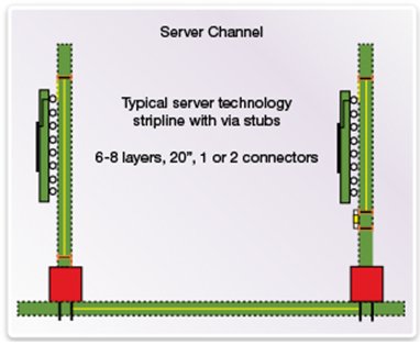
Figure 1 - Typical PCIe Server Channel
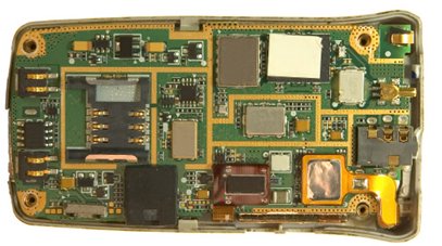
Figure 2 - Typical Mobile Phone PCB (<5 »)
Back in 2012, a new PCI-SIG Working Group was formed to reduce PCIe power and bring its protocol, programming models, and wide spectrum of designs to the mobile space. Ultimately the group decided to replace the “legacy” PCI Express PHY and utilize the MIPI Alliance’s M-PHY due to its proven power efficiency, range of speeds and acceptance by the Mobile industry.
The M-PCIe ECN provides dramatic power savings over similar PCIe designs. The Figure 3 shows how implementing the M-PCIe ECN impacts a typical PCIe Root-Complex to Endpoint device path. The upper PCIe protocol layers– the Transaction Layer (TL) and Data Link Layer (DLL) – can be unchanged in M-PCIe devices, ensuring that the PCIe programming models are unchanged
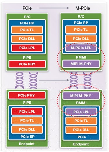
Figure 3 - M-PCIe vs PCIe Architecture
PCIe and M-PCIe devices have different designs for their Link Training and Status State Machine (LTSSM). The M-PCIe ECN developers strove to maintain similarity between the two state machines, but the M-PCIe version of the LTSSM is ultimately a different design. While this is a significant change to every PCI Express device, the modification was necessary to control the M-PHY's unique low-power states.
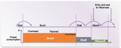
Figure 4 -
M-PHYs reduce power even further due to the relationship between their operating mode and individual burst transfers. In an M-PHY design, the PHY is only at its maximum power while actually transmitting. Upon completion of the burst transfer, the PHY drops to a much lower power “STALL” state and shortly thereafter into its lowest power “HIBERN8” state. By architecting for these rapid power state changes, M-PHY designers have minimized the amount of power consumed by active devices, thereby enabling long battery life.
To further reduce power consumption, M-PCIe systems can implement asymmetric links, which allow for different numbers of transmitters and receivers on a link. PCI Express forces the example device shown below to have 4 transmitters and 4 receivers to accommodate its need for 4 lanes worth of PCIe-to-cellular bandwidth.
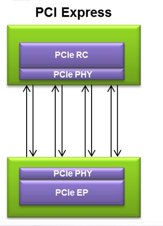
Figure 5 - PCIe Symmetric Lanes
Where PCI Express forced the example device to have an equal number of transmitters receivers to accommodate its maximum bandwidth in one direction, M-PCIe permits the device to reduce the number of transmitters to the required amount and in this case, only 2.
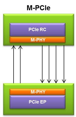
Figure 6 - M-PCIe Asymmetric Lanes
While the M-PCIe specification allows devices to consume less power than they would with the PCIe PHY, PCI Express offers higher speeds than M-PCIe. M-PCIe uses three of the M-PHY “gears” for signaling rates. In very general terms one can consider M-PHY Gear M as being the same bandwidth as the corresponding Generation (M-1) of PCI Express signaling. (See Figure 7)
| M-PCIe Speed | PCIe Signalling Generation | PCIe Speed |
| Gear 3 | Gen2 | 5.0GT/s |
| Gear 2 | Gen1 | 2.5GT/s |
| Gear 1 | N/A (Gen ½) | N/A (1.25GT/s) |
Figure 7 - M-PCIe vs PCIe Link Speeds
Thus selecting an M-PHY for its power savings both reduces the maximum trace lengths which can be used in an M-PCIe design and limits link speeds to less than what could be attained with PCIe’s “Generation 3” 8GT/s signaling – at least for today’s M-PHY Gear 3.
The M-PCIe ECN provides dramatic power savings for PCI Express architecture designs, which will enable their use in a much wider range of wireless and mobile devices than ever before. While the upper layers of the PCI Express protocol stack remain unchanged, it should be clear that architects and designers wishing to migrate system designs from PCIe to M-PCIe will have some challenges. Careful consideration of the issues described in this paper can minimize SoC designers' risk. Visit synopsys.com/m-pcie and follow the author at http://blogs.synopsys.com/expressyourself/ for more information.
