Nishant Madan,Gaurav Goyal, Syed Shakir Iqbal, Mayank Tutwani
Freescale Semiconductors India Pvt. Ltd.
Abstract:
Low power high performance designs have become a recent trend in modern SoC design community. Often multiple voltage domains are being created in order to cater the need of low power requirements and to communicate between these two domains level shifters are being used. However, these techniques are not completely effective as a part of the power saved by voltage islands is lost due to power consumed by these energy eating inefficient level shifter cells themselves. In this paper we propose high density low power architecture for level shifter cells that consumes ~ 5X lower powers with minimal compromise with performance.
Design
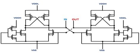
The proposed topology is based on the way of realization of a bi-directional level shifter using a single cross-coupled level-shifter rather than a two level-shifter based back to back connected architecture.
Generally, the back to back connected architecture suffers from huge power consumptions as the feed-back level-shifter is always on and switches with input signal needlessly.
To save this power loss due to needless switching we propose an architecture which uses a single feed-forward level shifter with switchable in/out ports so as to facilitate bi-directional operation based on a select signal.
The proposed topology is based on the way of realization of a bi-directional level shifter using a single cross-coupled level-shifter with switchable in/out port architecture.

Figure 1: Transistor level schematic for conventional bi-directional level shifter.
Major Source of Leakage power in Level Shifter:
Let’s say, when IN changes to 0.90V, M1 gets ON and from the previous cycle, OUT is at ‘0V’. So, M1 & M3 gets ON simultaneously and hence a direct path of current exists from VDDH to VSS and a huge current. This would get resolved once M4 makes the node ‘y’ at VDDH and M3 gets OFF.
Similar is the case with another half portion of the circuit.

Figure 2: Direct current path issue in conventional bi-directional level shifters.
To resolve the issue:
a) Reduce the timing window where both the M1 & M3 remain ON.
b) Avoid this unnecessary timing window where both the M1 & M3 remain ON.
Solution: Reduce the timing window where both the M1 & M3 remain ON.
a) This could be achieved by playing with the Sizes of the MOS’s involved, i.e. M1, M3 & M4 but this could impact the timing of the level shifter + gain is less and also not possible to reduce the timing window to ZERO.
b) Avoid this unnecessary timing window where both the M1 & M3 remain ON.
a) This can be taken care with the newly proposed architecture where only once during the operation, such condition occurs. While in the prior art this condition comes twice during the operation.
b)

Figure 3: Transistor level schematic for proposed bi-directional level shifter.
Operation
The port IN is associated with voltage level VDDL while port OUT is with VDDH.
1. Operation: IN to OUT, VDDL to VDDH (EN = 0).
During to low to high operation the EN signal is to be set as low.
M9 and M10 turn on passing the port IN to M11, M12 and M15.
For M11 and M12 the supply is connected to voltage level VDDL via M4 thus driving gate of M14 with logic level of VDDL.
The supply for the cross coupled level shifter also connected to high voltage level VDDH via M5.
If IN = 0 then, M14 is turned on and a logic low corresponding to VDDH is driven by M14 to M19 and M20 to the port OUT.
If IN = 1 then, M15 is turned on and a logic high corresponding to VDDH is driven M13 to M19 and M20 to the port OUT.
2. Operation: OUT to IN, VDDH to VDDL (EN = 1).
During to high to low operation the EN signal is to be set as high.
M7 and M8 turn on passing the port OUT to M11, M12 and M15.
For M11 and M12 the supply is connected to voltage level VDDH via M3 thus driving gate of M14 with logic level of VDDH.
The supply for the cross coupled level shifter also connected to high voltage level VDDL via M6.
If OUT = 0 then, M14 is turned on and a logic low corresponding to VDDL is driven by M14 to M17 and M18 to the port IN.
If OUT = 1 then, M15 is turned on and a logic high corresponding to VDDL is driven M13 to M17 and M18 to the port IN.

Figure 4: IN to OUT operation in proposed bi-directional level shifter.

Figure 5: OUT to IN operation in proposed bi-directional level shifter.
Results
The circuit was simulated:
- Voltage range : 0.9v to 1.32v & 1.32v to 0.90v
- Models – best, worst, typ, bpwn,wnwp.
- Timing parameters are measured at wcs, 150C.
- Power parameters are measured at bcs, 150C.
The circuit is an improvement over the original conventional cross coupled architecture in terms of huge reduction in power consumption with comparable area and timing parameters.

Figure 6: Delay comparison between proposed and conventional bi-directional level shifter.

Figure 7: Power comparison between proposed and conventional bi-directional level shifter.
Conclusion
In a multi core design with DVS , the supply voltages of different voltage islands there is an urgent need for bidirectional level shifters. The paper proposes a robust , high density , low power level shifter design which is capable of behaving as level shifter as well as voltage regulator. The idea has it in it to gain acceptance and large-scale use especially with the critical need for low-power & less area.
