By Sachin Kalra, Gaurav Goyal, Reecha Jajodia (Freescale Semiconductor India Pvt. Ltd.)
In shrinking technologies, all SoC’s have to work in multi modes and multi corners. So there is a tough challenge to meet setup and hold in all corners. Hold violation closure for a design involves Non-Si Hold closure (due to clock - skew) & Si Hold closure (due to clock and data noise). Non-Si Hold fixing is done by downsizing the existing logic or by putting more hold buffers in the path (primarily of Low drive buffers) while the Si-Hold fixing can be done by adding more buffers.
Since delay is reversely proportion to drive strength, low drive strength cell is chosen for hold fixing. These buffers are normal buffer cell with very less drive strength capability. These buffers have their own limitation. They are more noise prone cells. If there is huge timing violations, a chain of buffers are used and so local density becomes high for that IC.
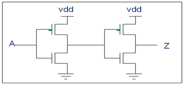
Below is the Fig. 1 which depicts a conventional Buffer design which has been used for the hold fixing.

Fig. 1 Conventional Buffer Cell Design
Contribution of noise from various elements in noise:
- 20-25% is from clock noise
- 50-55% logic data path elements
- 15-20% is from hold buffers added in the design
The conventional buffer design is not able to provide the desired delay needed for hold fixing & if a more low strength buffer needs to be used for more delay then that buffer suffers from noise. So, all these shortcomings led us to think of a new architecture of buffer which is capable for meeting hold timing without any impact in area, having a high delay with more noise immunity. i.e. a cell with more delay & with least noise prone so that it’s noise immunity also increases.
For the new proposed buffer cell design , there is a effort to increase the input ground cap so that Ground cap(Cg) which defines the ability of a net to resist a change in its state ----- ALWAYS Works Against Noise & for better noise immunity, deciding ratio is Ground cap/Coupling cap.
Transistors Ma, Mb, Mc & Md have been added which can also act as decap cells & also helps in providing the more delay to the circuit with increase of load at ‘A’ & ‘y’ nodes as can be seen from the below Fig. 2. Since, our aim was to fix hold violation. By this way we have increased the cell delay and also increase the noise immunity by increasing the input capacitance with the help of Ma & Mb transistors.

Fig. 2 Proposed Buffer Cell Design.
During designing of this cell we ensured there is no impact on area and power. Since the proposed cell has higher delay without any impact in area, local congestion issue can also be solved. The new architecture cell is designed such that it takes same area as the conventional cell but provides more delay & has inherit decap cells also which further helps in reducing dynamic IR drop.
Sometimes, there is a scenario where there is no space to add decap cells and a concern for IR drop is there, so such cells if get used in those regions for hold fixing can act as decap cells as well and hence serve DUAL PURPOSE without any extra cost. Uncertainty has reduced.
When ‘A” is at gnd i.e. ‘0’ : Ma & Md act as Pmos & Nmos decap.
When ‘A” is at vdd i.e. ‘1’ : Mc & Mb act as Pmos & Nmos decap.
There is no leakage from source to drain in default for decap, leakage is optimized. So, while talking about the whole design which is hold critical, same timing requirement is achieved by using less number of new architecture buffers. So in that way less congestion as compared to the same design with conventional buffer used. Below are spice simulation results for the comparison between the conventional design v/s proposed design at a cell level.

Table1. Spice results between conventional & proposed hold buffer
Design Results: We picked a design and did Noise hold fixing with:
- Run1: Conventional buffer only.
- Run2: Using proposed buffer only.
& below are the results:

Table2. Comparison between conventional & proposed hold buffer usage in a design
Due to the 20-25% saving in the number of hold buffers used, there is overall decrease in the leakage and dynamic power of the design while it is more for the individual cell comparison between conventional v/s proposed circuit as can be seen from the Table 1. Routing overhead is also less for hold fixing, less problem of local congestion. Area & power also gets saved due to less number of buffers used & since input capacitance has been increased which makes the circuit immune to noise.
Conclusion:
As per the above analysis, the proposed buffer cell is capable to fix the HOLD violations more efficiently as compared to the existing buffer cells & saves area, power & routing effort. Generally designers are chasing the high performance targets. All designs can use the proposed design architecture. Hold critical designs or congested design would be more beneficial from this circuit and also cycle time of any SoC can be reduced.
| Acronym | Explanation |
| SoC | System on Chip |
| IC | Integrated Circuit |
| Cg | Ground Capacitance |
| Post Si Hold | Hold fixing with noise |
