By Anurag Jindal, Sidhartha Taneja, Gaurav Goyal and Reecha Jajodia;
Freescale Semiconductor India Pvt. Ltd.
Scannability has always been a challenge and with the complex architectures, challenges gets multifold by imposing several limitations like HOLD closure, yield loss, silicon failures due to HOLD, scan architectures and complex scan-shift methodology.
The proposed Dual edge Flip-Flop architecture caters to eradicate the HOLD fixing by removing the HOLD violations completely in the design and helps in reducing the number of HOLD elements in the scan path to absolute ZERO which otherwise continue to eat unnecessary power/area/routing resources throughout the SoC life cycle after one time testing plus a very ROBUST and easy solution from the scan-DFT methodology perspective. The proposed architecture is Absolute ZERO HOLD architecture as far as the test path is concerned and a correct by constructs mechanism for the robust scan methodology.
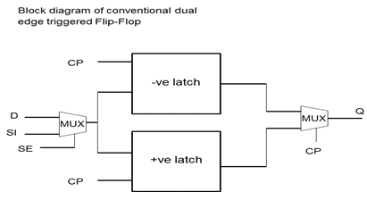
Below Fig.1 is conventional dual edge Flip-Flop architecture.
https://asicdigitaldesign.wordpress.com/2007/07/31/the-double-edge-flip-flop/

Fig. 1: Conventional Dual Edge Flip Flop Architecture.
Conventional Dual edge Flip-flop architecture is a normal dual edge mode of operation in the functional mode as well as in the scan mode. One of the most prevalent hold violations occur when there is no combinational logic between any two flip-flops. This can be seen very frequently in the scan chains. In order to resolve the HOLD violation either an extra delay is introduced between the two flops or the clock skew must be reduced. So, usage of conventional dual edge flip-flops in the design introduces lot of HOLD violations in the test/scan path and those need to be fixed which would eventually ends up in using lot of hold buffers which ultimately leads to wastage of area/time/power and still is susceptible to HOLD failures on silicon. So, the proposed architecture is able to fix the hold violations with inserting half-cycle clock cycle delay by the virtue of design in the scan path i.e. for the SI pin without impacting anything else.
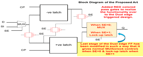
Proposed Circuit: Below Fig.2 is proposed dual edge Flip-Flop architecture.

Fig. 2: Block Diagram of the proposed dual edge Flip-Flop architecture.
Proposed Dual edge Flip-flop architecture is a normal dual edge mode of operation in the functional mode and single edge mode of operation in the scan mode with additional lock-up latch feature inbuilt. Intent is to make a dual edge functional Flip-flop when SE = 0, i.e. Scan enable is ‘0’ and single edge scan flip-flop with lock-up latch when SE = 1, i.e. Scan enable is ‘1’. This helps in reducing the HOLD violations to ZERO and makes the circuit very robust on the silicon and eases out the DFT scan methodology as well.
Transistor level implementation of the proposed circuit:

Fig. 3: Transistor level implementation of the proposed circuit.
Proposed circuit reduces to the Fig. 4 when SE = 0, i.e. Dual edge functional Flip-Flop functionality.

Fig. 4: Transistor level implementation of the proposed circuit when SE = 0
Proposed circuit reduces to the Fig. 5 when SE = 1, i.e. Single edge scan Flip-Flop with lock-up latch functionality.

Fig. 5: Transistor level implementation of the proposed circuit when SE = 1
Below Fig. 6 is the prior art implementation for the scan chains while using conventional dual edge Flip-flops.

Fig. 6: Scan chain depiction when using conventional dual edge Flip-Flop architecture
As per the Fig. 6, there is always a risk of missing lock-up latch between the scan chains of different domains with the source remains the same or can be different and a hold violation can pop up and failure on silicon can be seen.

Fig. 7: Scan chain depiction when using proposed circuit Flip-Flop architecture
As per the Fig. 7, it is clear that there is inbuilt lock-up latch with every flip-flop in scan chain. So, there is no way of missing lock-up latch and hence a very ROBUST solution from the silicon perspective.
Comparison Results and Conclusion:

So, proposed circuit is able to fix the hold violations with providing a half clock cycle delay by the virtue of design in the scan path i.e. for the TI pin without impacting anything else. ZERO effort involved in closing the scan path HOLD in the design which always ensures ZERO probability of Silicon failures due to HOLD and hence a very ROBUST and scan methodology as well. It also reduces the current scan DFT implementation involving multiple clocks to only ‘1’ scan clock definition which further eases out the DFT effort during identification and defining the scope of clocks during scan. This also eliminates the requirement for lock-up latches in the scan path.
| Acronym | Explanation |
| SoC | System on Chip |
| CG | Clock Gating |
| DFT | Design for Test |
| OCV | On - Chip Variation |
