NVM OTP in UMC (180nm, 153nm, 110nm, 90nm, 80nm, 55nm, 40nm, 28nm, 22nm)
Agile Design for Hardware, Part II
David Patterson and Borivoje Nikolić, UC Berkeley
EETimes (7/30/2015 07:00 AM EDT)
In the second of a three-part series, two Berkeley professors suggest its time to apply Agile design techniques to hardware.
We asked readers of Part I to guess the cost of a prototype run of 28 nm chips, as Agile development relies on a sequence of interim prototypes versus the One Big Tapeout of the traditional Waterfall process. Here are the results:
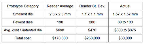
The surprisingly low manufacturing cost of prototype chips—one fifth the readers’ estimate—means Agile development is eminently affordable, even for academics. (See www.AgileSoC.com for more evidence.) It also calls into question the current high cost of designing SoCs using the Waterfall process. Having established Agile’s viability, based on our experience we propose four guidelines to lower development costs.
![]() |
E-mail This Article | ![]() |
![]() |
Printer-Friendly Page |
Related Articles
- Agile Design for Hardware, Part I
- Is Agile coming to Hardware Development?
- Dealing with automotive software complexity with virtual prototyping - Part 2: An AUTOSAR use case
- Optimizing embedded software for power efficiency: Part 2 - Minimizing hardware power
- Optimizing High Performance CPUs, GPUs and DSPs? Use logic and memory IP - Part II
New Articles
- Optimizing 16-Bit Unsigned Multipliers with Reversible Logic Gates for an Enhanced Performance
- How NoC architecture solves MCU design challenges
- Automating Hardware-Software Consistency in Complex SoCs
- Beyond Limits: Unleashing the 10.7 Gbps LPDDR5X Subsystem
- How to Design Secure SoCs: Essential Security Features for Digital Designers