By Eric Esteve, IPnest
June 2018
This Position Paper describes a family of Power Management IP solutions integrated by Dolphin Integration’s customers into their SoC to drastically improve Energy Efficiency (EE). SoC performance metric is changing, moving from pure performance metric (GHz or MIPS) to performance efficiency and minimum power consumption. This new metric, already crucial for IoT or mobile devices, is becoming key in various applications, like automotive, embedded or space. We will show that a SoC design team may leverage Silicon IP to implement complex power management and can greatly benefit from technical support given by experienced engineers to improve time-to-market (TTM) and project development cost. This paper was prepared by IPnest and sponsored by Dolphin Integration, but the opinions and analysis are those of the author.
Energy Efficiency is Becoming Critical in the Semiconductor Industry
The power consumption generated by complex chips was not a real issue when the system could be simply plugged into the wall to receive electricity. The most important feature was raw performance, expressed in GHz or MIPS, and was used to sell PC to end-user, for example. Nevertheless, with the huge adoption for wireless mobile devices in the 2000 and later, the metric tends to change. For battery powered devices, the time between two battery charge became almost as important as the MIPS power delivered by the phone/smartphone.
Now, let’s take a step back and consider the semiconductor (and electronic) industry as a source of power consumption, including servers, storage, high power computing (HPC), wired networking, 4G and 5G base stations, all very demanding of high performance, as well as consumer, automotive, etc. The Semiconductor Industry Association (SIA) and Semiconductor Research Corporation (SRC) have released in 2015 the report “Rebooting the IT Revolution: A Call for Action”, including this graphic:
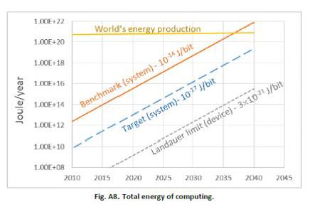
Figure 1: Total Energy of Computing (Source: SIA 2015)
The status is crystal clear, considering the power consumed by data center (based on state of the art system in 2015), the energy burnt in computing only would equal the world’s energy production in 2037, or less than 20 years! That’s why the survey is titled “A Call for Actions”. Which is true for data center is also true for other applications like automotive and obviously IoT, even if it’s for several reasons. We can admit that most of IoT IC will be devices, or edge systems. In fact, the need to include computing power (CPU or DSP) into edge systems is now accepted by the industry, as moving data up (to the IoT master) and down (once the data has been processed) is clearly not the right choice. We can mention unacceptable latency for critical systems like autonomous cars, or global system efficiency in every case: does it make sense to send simple data miles away, using high speed links and expensive base station or network, just to process an addition or any other simple math function in data center?
In this paper, we will address the multiple applications integrating IC developed in mature technology nodes (by opposition with the most advanced nodes like 14/16 nm, 10 nm or 7 nm), in various segments like IoT, automotive, consumer, for systems which may or may not be battery powered. We will set the goal: decreasing an IC power consumption while keeping performance, development lead time and costs with the same IC with no power management effort, identify the potential issues (noise margin, crosstalk, etc.) and review the solutions proposed by Dolphin Integration to reach this goal with zero impact on TTM, cost and correct functionality.
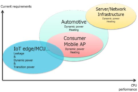
Figure 2: Power Issues by Application (Source: Dolphin Integration)
Various Solutions to Decrease SoC Power Consumption
As mentioned above, the wireless mobile industry has pioneered the power management techniques since the years 2000’s. Design team in charge of application processor SoC (like TI with OMAP, followed by Qualcomm, Samsung, Apple and many other) have implemented power management strategy at system level, the phone. It’s important to notice that the power management techniques were so complex that they have quickly realized that an external device was needed on top of the internal power management features, the Power Management IC or PMIC. The various solutions reviewed here will be implemented inside the SoC, with no need for PMIC, as the goal is to keep the cost the same, or at lower level, that it was before implementing power management.
We will review the various techniques leading to decrease the SoC power consumption.
Power Domains Management
Defining power domains is the first step to consider, before implementing any specific power network IP or power distribution strategy. Keep in mind that the power domains will be defined in respect with functional blocks in the SoC. One functional block may involve different type of cell, like a CPU and a block of digital standard cells, together linked with SRAM memory. These blocks may get the power from different supply sources, at different voltage levels.
The various domains defined, the goal is to implement the specific power distribution to a specific power domain, and to create power islands. Each domain can be isolated from the rest of the SoC and powered down (or up) with no effect on the other power domains. We will see later in the paper how to deploy this power management strategy.
Dynamic Voltage Frequency Scaling (DVFS)
The dynamic power consumption is expressed by the formula:
PT = Cpd x Cpd x VCC 2 x fI x NSW
Where:
- PT = Transient Power consumption
- VCC = Supply voltage
- fI = Input signal frequency
- NSW = number of bits switching
- Cpd = dynamic power dissipation capacitance
The combination of supply voltage and frequency has a cubic impact on total power dissipation because dynamic power consumption has a quadratic dependence on voltage and a linear dependence on frequency. An intelligent power saving solution would reduce operating frequency and, at the same time, reduce the supply voltage.
The main idea is to scale the supply voltage as low as possible for a given frequency while still maintaining correct operation for certain functions. The voltage can be dropped only up to a certain critical level, beyond which timing faults occur.
When applying per-function DVFS approach, assuming that per-function power/clock domain have been defined and additional circuitry implemented, the SoC global power consumption can be severely decreased, while keeping the performance the same, or better, for the functions running as usual when the others are kept quiet (ie: lowered voltage).
The dynamic voltage and frequency scaling (DVFS) has been widely adopted by laptop computers, servers, and mobile devices to conserve energy, while DVFS is still at a certain early age for other applications (automotive, consumer, …). According to experimental results, DVFS has significant potential for energy saving. DVFS is just one of several methods to control dynamic power consumption in CMOS circuits. We must keep in mind that its usage brings a set of verification and implementation challenges, but DVFS is very efficient to decrease the SoC power consumption in active modes.
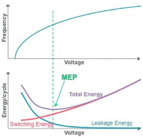
Figure 3: Energy (dynamic and leakage) vs Voltage
Near Threshold Voltage
Total power is a combination of static or leakage power and dynamic power. As the voltage is dropped toward the transistor threshold voltage (Vt), switching power decreases but at the same time leakage current increases. This means the optimal combination between leakage and switching power has to be found as shown on Figure 3.
Near Threshold Voltage (NTV) will be selected in the voltage range offering the minimum of energy (see Figure 3) while keeping the functional domain working. NTV is an excellent power management technique and give very good results in term of Energy Efficiency (EE) as we can see on Figure 4. These results come from measurement made on Intel Pentium and we can notice that, for 0.45 V (near threshold value), EE efficiency reaches 5830 Mips per Watt, to be compared with EE at nominal voltage (1.2 V) of 1240 Mips/Watt. The first drawback can be seen on the same figure: at nominal voltage (1.2 V) the chip frequency reaches 915 MHz, whereas at NTV (0.45 V) it’s only 60 MHz.
NTV gives excellent results (power consumption and Energy Efficiency), specifically in sleep or in triggering modes, as SoC doesn’t need to run a full performance in such modes, like for example IoT edge computing or Always-on sensors.
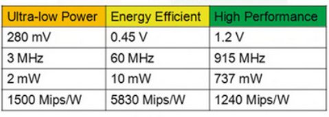
Figure 4: Energy Efficiency vs Functional Voltage
Other techniques: body biasing, GALS, …
GALS technology is used for maximum clock domain management efficiency. Cross-clock boundaries should be instantiated using unidirectional bi-synchronous devices (like FIFOs), allowing for optimal latency with no handshake required. Clock boundaries can be partitioned along any link within the interconnect and the GALS elements can be bypassed for synchronous operation.
Power and voltage domains are separated by an electrical isolation layer, and individual functional blocks should be turned off using disconnect techniques. Retention registers should be inserted when specific functional blocks must retain state when the power domain is shut off.
In summary, GALS is an efficient but very demanding (at engineering level) power management approach, and it involves specific design knowledge and trick to apply existing EDA tools. As a result GALS, should be considered after having implemented other techniques like clock gating, power domains management or DVFS.
Body Biasing is a chip management technique which can be used to decrease power consumption or increase performance, depending of the substrate bias voltage applied in respect with the voltage applied to the active part of the chip. Although you can theoretically apply voltage to any substrate, including bulk, body biasing is mainly used with Silicon on insulator (SOI) wafers. Fully Depleted SOI (FD-SOI) technology has seen traction since a couple of years and several foundries (Samsung, GlobalFoundries) and IDM (STMicroelectronics) are offering ASIC capability in 28 nm, 22 nm and 14 nm. ASIC design targeting FDPower SOI technology is not necessarily more complicated than on bulk, but the ecosystem is currently working to offer EDA tools and IP supporting body biasing. Nevertheless, body biasing on FD-SOI is an excellent approach to decrease SoC power consumption.
Various Power Issues Impacting SoC Integrity
To meet the aggressive power budget targets, the design team may have no other choice than to operate at extremely low power levels. The direct impact is to increase the critical signals’ susceptibility to electromagnetic (EM) crosstalk effects.
Because a low-power SoC has much smaller noise margin, switching activities can cause ringing on the power delivery network (PDN) and adversely affect the chip’s performance.
In today’s design, clock and power distribution networks are the main contributors of an integrated circuits failure mechanism, such as jitter, clock skews, electromigration, coupling noise and power distribution droops. Hence, both performance and risk aversion are dependent on the robustness of clock and power distribution network design, making accurate modeling of inductive and magnetic effects a fundamental requirement.
For example, consider a power distribution network that is feeding a digital block with high current demand and very fast switching activity (i.e., drawing high current peak in very fast transients). Such an activity would result in ringing on the power distribution network (PDN) that is proportional to the inductance (L) and the rate of switching activity (di/dt). As switching activity increases, the magnitude of the ringing will increase, as well as the noise level on critical and/or sensitive high frequency or very sensible analog signals, through coupling with PDN. An other challenge is the low frequency noise generated during mode transitions which may create functionality issues.
Power consists of dynamic power and leakage current. Dynamic power is dependent on total load capacitance, supply voltage and operating frequency. Lowering any of these parameters can result in lower dynamic power. But a common design methodology for PDN is to insert enough decaps to filter the spikes on the network due to simultaneous switching noise that can result in large current spikes at the clock edges. Leakage power is caused by the current path between supply and ground when NMOS and PMOS channels of a CMOS gate are simultaneously turned on during the rise and fall time of the input signal.
To make sure that your SoC design will not be impacted by power or clock related issues, you will have to benefit from technical support given by experienced engineers. Like with analog design, nothing can replace experience, and Dolphin Integration engineers have been trained and know when and how implement power management techniques, thanks to their design activity on chips developed for customers.
Implementing Power Management IP in Customer’s SoC
Power domain identification
We first need to define the SoC power architecture as this architecture can strongly vary with the functional architecture. This will be the first task for the designer to identify the various functions belonging to the same power domain. This power domain is not simply defined by voltage, but in respect with the functionality of the various blocks expected to be part of the same task in a given power mode. Assuming this power architecture has been defined, the SoC is now partitioned into N domains (N being in the range of 5 or even more). Each of these domains can be independently monitored in respect with the voltage supply (Vdd1 to VddN) and the designer can implement power distribution and the power activity control at SoC level, in this case independent power grid for each of the Vddn. At this stage, Dolphin Integration will propose technical support given by experienced engineers, the SoC Architectural Experts (SAE). These engineers are not simple FAE, they have also managed power management implementation internally, in SoC developed inhouse by Dolphin Integration for customers (design services) or internal usage. Dolphin Integration power management IP supports up to 128 power domains.

Figure 5: Power Domains in a SoC (Source: Dolphin Integration)
Power gating, control & distribution
The various power domains have been defined by the design team, helped by Dolphin Integration expert engineers, it’s now time to define the SoC power architecture, and to implement the power and clock distribution in the chip. Each power domain should be powered, the power gating inserted to control this domain. Dolphin Integration has developed patented Power gating device of power islands (named CLICK), as well as a voltage Domain interfacing Cells (VDIC). Dolphin Integration experts will help the team to select the right voltage regulator within a large variety of voltage regulators (LDOs and DC-DCs) organized as a library of pre-configured silicon IPs.
Dolphin Integration also proposes an Over-voltage Protection Module to support up to 5.5 V. To provide the clock to this domain, the customer will benefit from an ultra-low power clock IP (named Gamma). Using the right clock and power distribution device is critical, as “clock and power distribution networks are the main contributors of an integrated circuits failure mechanism, such as jitter, clock skews, electromigration, coupling noise and power distribution droops”, as above mentioned!
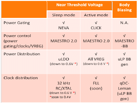
Figure 6: Power Gating, Control and Distribution (Dolphin Integration port-folio)
At chip level SoC designer will select controlling power switches, VREG or Body Biasing generator and clocks, all part of the power network IP port-folio, to power the SoC core. The implementation of the SoC power mode control is straight-forward thanks to a modular IP solution (named MAESTRO). These cells are modules carefully designed, integrating built-in conflict management to prevent failure during SoC operation and transition.
If the SoC is designed for Native Threshold Voltage (NTV) or DVFS operation, Dolphin Integration IP portfolio has been designed with native NTV and DVFS support, in sleep or active mode, as shown in the Table below (Figure 6).
The consistency of this complete Power Management IP offering of Dolphin Integration is ensured through the compliance with structural and assembly rules (named DELTA rules). SoC designers may leverage inhouse development of their own VREG through the adoption of similar rules to enable a seamless SoC integration.
Dolphin Integration Power Management IPs allow providing on-SoC power delivery and power mode control, the main goal is to provide the various IP and technical support from experts for safest design of Energy-Efficient (EE) SoCs. Because of this expertise from Dolphin Integration engineers, there is no doubt that this SoC design will be fastest compared with the development schedule of the same SoC, when power management is integrated for the first time by a design team with no support. Dolphin Integration is proud to guarantee this fastest TTM to customer deciding to build energy efficient SoC to attack emergent market like IoT as well as mature market (automotive, consumer, …) where the need for energy efficiency is becoming crucial.
Figure 7: Complete set of Power Management IP (Dolphin Integration port-folio in a SoC)
Clock distribution
Dolphin Integration clocks IPs allow implementing an always-on power domain capable to operate at 32 kHz Near Threshold Voltage. The clocks source may be crystal-based or RC-based depending on the targeted clock accuracy. RC and XTAL oscillators may also be combined to as to ensure a fast start-up on the RC oscillator and then a switch to a XTAL oscillator once it is operational.
As the current of RAMs in retention scales with voltage, targeting an operation of the always-on power domain as close as possible to the minimum data retention voltage of the RAM (MDRV) ensures the lowest power consumption in SoC sleep mode. The library of voltage regulators from Dolphin Integration includes an ultra-low quiescent voltage regulator with a programmable output voltage down to 0.6 V while consuming no more than 150 nA with its voltage reference included.
Expertise Needed to Efficiently Implement Power Management
As already mentioned, but it’s important to re-assess the point, expertise is key when dealing with power (control, gating or distribution). Those who have been involved in SoC digital design integrating some analog functions know that you must take very special care when integrating analog! I am not only talking about the analog design itself, clearly a task for expert only, but also about the clocking and power distribution, as well as signal integrity protection. Power management implementation is very similar, only the know-how and expertise can guarantee first time right design.
That’s why Dolphin Integration, on top of technical support given by PM experts, try to further help their customers by developing proven methodology, and this translate into the development of EDA tools specific to power management with the goal to deterministically select the right power architecture and IP components. These are today in beta version and address all the power management implementation steps:
- PowerArchitect™ allows exploration of various power architecture and selection of the optimum operating point
- PowerDesigner™ is an automated tool for generating the top UPF, top RTL and the RTL of the ACU built with MAESTRO modules UPF design from top RTL
- PowerVision™ is a power integrity driven SoC simulation tool
Dealing with power management and distribution is a very demanding task, and very tricky! Unlike digital design, there is no Verification IP (VIP) and running analog simulation (SPICE) is not possible when developing a complete SoC (too large). Moreover, could we ask to a digital designer to manage analog simulation? But taking a slightly wrong decision (remember, we are not in the digital world “1” or “0”) when selecting a power cell may impact the signal integrity of a critical signal, maybe far away. The best way to safely implement power management in a SoC is to ask for the know-how of engineers who have built expertise in this field, and will help to create the best power architecture, and implement power management so your SoC will become energy efficient.
Conclusion
High chip power consumption is now a real concern for chip makers, in any segment of the electronic industry. When complex power management solutions were only implemented in wireless mobile applications in years 2000’s, it’s becoming mandatory to implement these solutions for IoT, automotive or consumer applications.
But this task -implementing efficient power management in a SoC- can be perceived as complex and risky for a SoC architect doing it for the first time. Complex because he is discovering various functions, mostly analog, and he was not trained to select and implement it in a SoC. That’s why the risk is real to impact the design schedule when making the wrong choices, leading to miss the Time-to-Market (TTM), a major risk in this fast-moving industry.
Dolphin Integration has developed a complete library of cells serving to implement power management in a SoC (voltage regulator, power domain interfacing calls, power distribution, clock distribution and so on). Dolphin Integration is not just selling this library, but act at the beginning of the project to help the design team to define the SoC power architecture and implementation strategy, by offering technical support from well experienced designers, the SoC Architectural Experts (SAE).
That’s why Dolphin Integration can proudly claim that their power management solution improves time-tomarket (TTM), project development cost and Bill of Material (BoM) cost. Selecting Dolphin Integration’s power management IP will not only help reaching power consumption target, but also keep the SoC development schedule and cost within the specified goal, thanks to the excellent technical support given by Dolphin Integration’s engineers during the power management implementation in the SoC.

