By Rajesh Uppuluri and Ramesh Devani (eInfochips)
Introduction
With advanced technology nodes, the SoCs are growing in density and gate count. This creates challenges regarding the testability, and more importantly, the test cost. The design complexity and size brings in the need for an advanced scan architecture to allow flexibility in adopting reduced pin count testing without increasing the overall test data volume and test time.
When the design size begins to reach the capacity of ATPG (Automatic Test Pattern Generation), a hierarchical approach for structured DFT implementation and pattern generation provides several advantages. This paper describes the detailed aspects of hierarchical DFT, with Shared Scan-in methodology using DFTMAX, the low pin count solution from Synopsys. The technique of sharing scan-in data between identical and non-identical cores, known as broadcasting, was employed to reduce the cost.
Design Details

Scan testing Requirements
Work within the following scan constraints/requirements:
- Should meet test coverage goals along with diagnosis in compression mode.
No compromise on the number of Scan-ins/Scan-outs as we are targeting high X-tolerance.
- Scan insertion should adhere to the physical hierarchies for a seamless flow.
Compression logic is to be placed inside the CORE to reduce congestion.
- Compression to be implemented for different blocks
However, we shall still have the flexibility to test the blocks individually.
- Scan pin requirements should be satisfied within the total number of IOs available.
Imposed a significant challenge as not enough pins on our design for all compressors.
This creates challenges related to the testability, and more importantly, the test cost. In addition, the SoC has multiple instances of many modules.
This approach helped us reduce the test data volume/test pin requirements and retain full observability on the scan outputs. This ensured that test coverage and the pattern count met the target goals.
DFTMAX
DFT in complex designs are always challenged to meet criteria between tester memory size, fault coverage, and low pin count. In scan compression tools such as DFTMAX, combinatorial techniques are used for the compression circuit design where a specific number of pins are needed to achieve 100% X-tolerant compression.
DFTMAX Compression
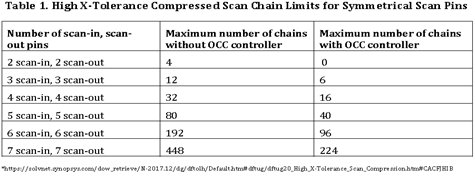
For large designs with specific chain length, DFTMAX yields a high number of scan chains requiring a larger number of scan input and output pins. Table 1 highlights the pin requirement for the specific number of scan chains needed to achieve 100% X-tolerance when using a symmetrical scan input and output pin configuration. As the number of scan chains increase, a larger number of scan pins are required and it deteriorates in design with an OCC controller.

Considerations that informed our choice of architecture included the following points:
- Generally, for each core, the number of scan input and output channels is much lower than the number of available scan I/O ports at TOP. There is room for multiple cores to be tested in parallel.
- The total number of the core's scan channels is typically several times larger than the number of scan I/O ports.
Input Sharing (Broadcasting) for cores
In our SoC, a large number of identical cores are present. By effectively sharing the SI pins of these cores, the number of SI pins required are reduced at the TOP. These uninitialized SI pins can be used to test other cores in parallel, saving the test time.
This important feature provides design testability with reduced pin count, not only for identical codecs but also for any non-identical codecs. This means that with "n" codecs shared, we would require log-u(n) (rounded to next integer) pins for selection.
Uniform sharing of scan inputs ensures that TetraMAX can perform its own optimizations to improve ATPG efficiency for designs that utilize identical cores.
Chosen DFT strategy
- Hierarchical DFT approach: complete bottom-up flow
- Massive investment on flow automation (compression, MBIST) for sub-chip management
- DFT insertion on 7 out of 9 blocks was executed with compression
- Intensive effort spent to have all sub-chips clean and violation-free
- Full ATPG (stuck-at, transition) and MBIST patterns validation
- Formal proof (Equivalence Checking with Formality)
These actions allowed us to lighten the effort at top level and achieve DFT closure more rapidly.
Implementation challenges
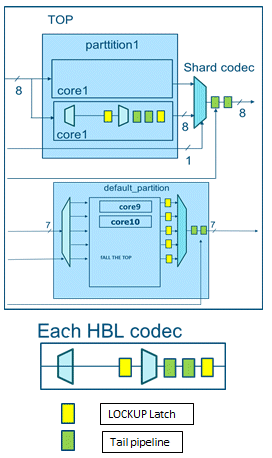
To meet the pin requirements, we partitioned the design into three. Within each partition, all the codec I/Os were shared. Each partition had its dedicated I/Os. We went with the reasonable assumption that flop count is proportional to design size. Therefore, partitions were done based on the flop count and not on the total number of gates. Each partition had a similar flop count. The underlying objective of partitioning the design was to completely switch off shift and capture clock of the selected partition and still able to generate patterns for remaining partition/s.
Shared scan-out from each partition should be compacted down to the required scan-out to meet low pin count requirements. For high X-tolerance codecs, additional scan-inputs are needed for the output sharing compressor to observe required codec-output during X masking cycles. The number of additional codec-select scan-in pins is ceil (log2N) where N is the number of codecs.
In an OCC controller flow, the clock chain is a special scan segment that provides control over the at-speed capture pulse sequence generated by the OCC controller. All the OCC clock chain bits are required during each capture phase and hence every bit is a care bit. The clock chain is constructed as an external clock chain with a dedicated test input pin and a dedicated test output pin, that are excluded from compression and so seen as an additional scan chain. Hence, the dedicated clock chain scan-in signal reduces the number of scan-in signals available.
Scan insertion script with scan-in sharing at the Top-level
current design TOP
read design // remaining TOP
read test model {CORE1 CORE2 CORE3 CORE4 CORE5}.ctl
set dft config -scan compression enable
current_dft_partition CODECA
set_scan_compression_configuration -integration_only true
set_scan_compression_configuration -shared_inputs 9 -shared_outputs 8 -input 8 -output 8
set_scan_configuration -chain_count 8
//ScanIn/out definitions for the partition
current_dft_partition CODECB
set_scan_compression_configuration -integration_only true
set_scan_compression_config -shared_inputs 15 -shared_outputs 11 -input 11 -output 11
set_scan_configuration -chain_count 14 -test_mode Internal_scan
set_scan_compression_configuration -max_length 350
current_dft_partition default_partition
set_dft_configuration -scan_compression enable
set_scan_configuration -chain_count 5 -test_mode Internal_scan
set_scan_compression_configuration -inputs 7 -outputs 7
set_scan_compression_configuration -hybrid true
In the hierarchical adaptive scan synthesis (HASS) flow, scan compression logic is placed at the block level, and all cores with scan compression logic are integrated at the chip level. This approach helps reduce the routing congestion prevalent in SoC designs.
UnCompression mode with Broadcasting (input sharing) connection
The cores are configured in Bypass mode where the Compression is bypassed. In this mode, there exists a broadcast connectivity from the same SI pins to multiple identical codecs from the TOP I/Os.
We have used the DFTMAX Shared scan inputs/outputs (I/O) CODEC architecture for our design to reduce the test time. In addition to reducing the test time by implementing the compression architecture, DFTMAX Shared I/O CODEC also shares the inputs and outputs of the different compression structures in the design and addresses the scan channel limitation at the top level.
Conclusion
To overcome the growing challenges related to testability and cost of testing that result from design complexity and size, it is effective to use a hierarchical approach for structured DFT implementation and pattern generation. Using the method outlined above, we were able to successfully implement shared scan-ins, which enabled us to perform all partition's testing within existing pin count. As the flow was completely automated within DFTMAX/TetraMAX, we also benefited from a quicker TTR.
Authors
Rajesh Uppuluri is Member of Technical Staff engineer at eInfochips. He holds a Master's degree from BITS, Pilani, India. With over 10+ years of experience in DFT implementation and ASIC Tool Development, he focuses on delivering complex SOC ASIC products in lower technology nodes for eInfochips’ customers. He is an expert in DFT, ATPG, and low power solutions.
Ramesh Devani is working as an ASIC DFT Manager at eInfochips, an Arrow company. He has more than 12 years of experience in ASIC DFT. He has an experience of working on various technology nodes, from 180nm to 14nm, handling different DFT tasks. He manages a medium sized team of engineers.
