By Ramesh Devani, Piyush Chaniyara, Khushali Dudhagara , Denish Thummar, Maulik Bhoraniya (eInfochips)
Abstract
In deep sub-micron technology nodes (180nm and lower), the design process of SoC becomes complex by integrating multiple IPs having different functionalities on a single chip. In such a scenario, tracking and controlling of the area becomes a key challenge.
In most SoC, the memory occupies major area. Circuitry added to test that memory creates area overhead. After each pass of DFT, area increases with the test logic and it becomes very difficult to control it. In this article, tracking, and controlling the area is discussed.
1. Introduction
DFT logic circuitry is added during the design process of SoC to ease its testing on ATE (post-manufacturing). Such logic circuits are added to the design without affecting the functionality of SoC. After each pass of the DFT, some area gets added to the design because of the DFT logic circuit.
This DFT circuitry overheads the area for a chip. Minimizing and controlling the area by keeping its track is very essential for a DFT engineer. In this article, the area increased by each individual component is discussed with details on how one can keep track of the same.
In general, the flow of DFT logic insertion includes pre-DFT circuit insertion, MBIST and scan insertion. During pre-DFT circuit, additional circuitry like TAP, muxes, control registers and wrapper circuitry are inserted into the SoC design for ease of validation on ATE.
During MBIST, a tool inserts another TAP, BIST/BIRA controller, memory interfaces that include observing flop, repair code muxes, pipeline flops, fuse box and more.
In scan insertion, we usually insert compressor and decompressor, wrapper, shared codec, test points, auto fixes, etc.
Section 2 of the article describes how the area is increased during pre-DFT circuit insertion & MBIST, with detailed discussion on the area of MBIST component and calculations. In Section 3, area increment during scan and how to control it is discussed. In Section 4, the area track during each pass is shown with practical results.
2. Post-MBIST area overhead & calculation
Major increment of area during MBIST is because of inserted controller and interface. The number of controllers depends on the type of memories in the design, i.e. RAM & ROM. We have different controllers for the memories working on different frequencies. For the SMRD, the controller has a different configuration than normal BIST controller as it controls the fuse box initialization and logic. The fuse box size depends on the redundancy, i.e. the number of redundant columns or rows.
Scenario: The memory cell named AB111CD26EF11W00256G031H is to be replaced with redundant cell AB111CD26EF11W00256G0032H having one redundant column. Now the fuse size will depend on the number of columns. Here, the memory cell has 31 columns, so it will require fuse box sized 5 register. It follows a simple formula:
Minimum (2N > Number of column). For this memory, the fuse box size will be the minimum size of N.
Consider a design having 30 memory cells with same column size – 32. During MBIST, 150 registers will be added, named with *fuse*. For the 40 nm technology node, scan flop’s area would be around 4.572288 µm2 .
-
Total area overhead = 4.572288 * 150 = 685.4832 µm2 .
The controller area for a design having 6 memory cells, 2 controllers and 21 interfaces for 40nm technology will have an area of around 12354.9 µm2 .
2.1 Interface
The memory is always surrounded by some test logics. It includes observe flops, repair code mux, fuse box decoder, bypass logic, pipeline stages, etc. We will discuss a few of the testing logics on the output side.
The default-control switch (of command SET San Logic) option is provided to mux the scan/non-scan cell output to the memory data output. This is helpful in testing logic on the output side of the memory during scan test. The tool inserts one mux for each data output. It connects one input of the mux to memory data output and the other input of the mux to the newly inserted scan/non-scan cells. The mux is controlled by the test_mode signal as shown in Fig. 1 below.
Now, let us look at interface and shadow logic of memory:
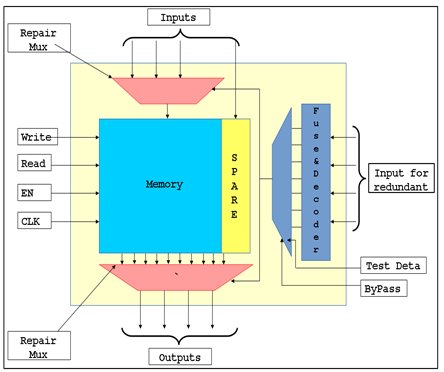
Fig.1: Memory with spare column and decoder logic
The bypass logic created by command SET SCan Logic is placed in a hierarchical block called memory_name_bypass.
2.2 Observe cells
The observe cells for address, data, and control signals are always processed in the order of the smallest signal first, unless all of the signals are specified through user-defined values.
Observe cell calculation:
Average = Total Number of Input Cells ÷ Number of output cells
Cells for Group X = Integer part of (Size of Group X ÷ Average)
| Signal | Number of Signal Lines |
| Address | 4 |
| Data | 8 |
| Control | 2 |
Average compression / cell
= Number of (address lines + data lines + control lines) ÷ Number of data lines
= (4 + 8 + 2) ÷ 8
= 1.75
Processed in the order of smaller number of signals first. Also, note that the results that yield decimal values will be truncated.
Control_observe cells = 2 ÷ 1.75 = 1
Address_observe cells = 4 ÷ 1.75 = 2
Data_observe cells = 8 - (1 + 2) = 5
2.3 Pipeline registers
If the model is found to be synchronous, and it conforms to the requirements, it is internally converted to a full-speed version. The tool processes read/write cycles of the memory model and converts them into single-cycle operations. Once all memories are verified, the tool determines the proper pipeline depth and automatically defines the pipeline in the tool environment. The tool adds pipeline stages to meet timing requirements for high-speed testing.
Depending on the range of address bit and data bit, pipeline stages will be added. Pipelines added in the periphery of the controller and the memory are shown in below figure with boxes highlighted in red.
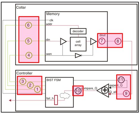
Fig.2: Insertion of pipeline stages
We can calculate area for observe flops and pipeline registers by taking reference of scenario 1.
The total area overhead during MBIST can be represented by the below chart for memory size 0512x032. We can see that the memory collar area is reduced in SMRD Memory BIST. This happens as the bypass logic area is moved from memory collar to SMRD.
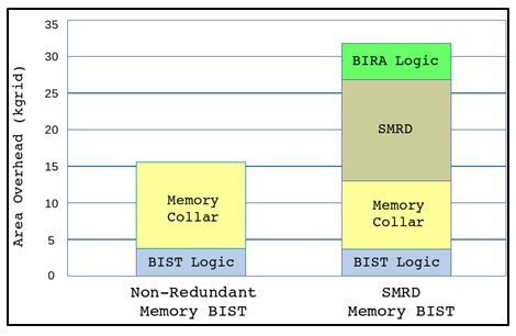
Fig.3: Difference between Non-Redundant & SMRD MBIST (Kgrid is group of cells)
3. Post scan insertion area overhead and calculation
Increment in the area during scan insertion primarily results due to components added to make the circuit testable. This logic can be compression-decompression, latches, wrapper around cores, pipeline register, test points, etc. Let us look at each component.
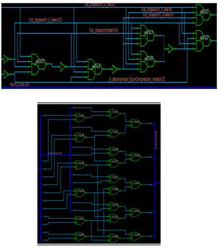
Fig.4: Decompressor-compressor logic for design having 50 scan cells
Scenario 2, consider the design having the number of scan flops as 22441. For the 40nm technology, compression and decompression will increase area of 1942.79 µ . It is about 1% of the design area. Test point insertion and wrapper logic area will add the overhead on it.
The lockup latch is added in the scan chain by the tool when a designer decides to use the clock-mixing feature in the design. The tool inserts this latch to prevent the hold scenario. This feature helps in scan chain balancing but it adds the area overhead and scan chain reordering also becomes difficult in this case.
Consider a design which has multiple clocks. If pipeline stages are added (head and tail), then the tool will insert the lockup latch at starting and ending of the scan chain as shown below in figure 4.
The total number of pipeline registers would be equal to #input stages x Scan in + #output stage x scan out.
The total number of the latch in compression would be equal to #scan chains - #scan chain driven by pipeline clock.
(# shows Number of)
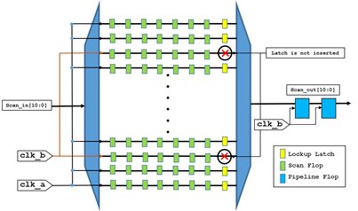
Fig.5: Lockup latches inserted at the end of the scan chain
As shown above in figure 5, the flops are driven mainly by two clocks clk_a and clk_b. The pipeline flops are driven by clk_b. The lockup latch will be inserted when there is clock domain change. So, here the latch is added at the end of the scan chain which is driven by the clock - clk_a - while the latch is not inserted in remaining chains. By observing this, we can conclude that to reduce the latch insertion in such cases, we must choose the pipeline clock that drives the most scan chains. We can calculate the area as per the calculations shown in Scenario 1.
4. Practical result of a design at 40nm technology node
1) Pre-MBIST:
| Block | Gate Area Single Block (a) | # Gate Single Block (b) | SRAM Area Single Block | # Block Instance (d) | Total Gate Area | #Total Gates |
|
| [um2] | [gates] | [um2] | [pcs] | [um2] | [gates] |
|
|
| a*X*Y |
|
| a*d | b*d |
| XYZ | 2010879.23 | 4152037.21 | 1422880.24 | 2 | 4021758 | 8304374.42 |
2) Post - MBIST:
| Block | CTRL | INTERFACE | SRAM Area With RD Single Block | # Block Instance (d) | Total Gate Area | # Total Gates |
|
| [um2] | [gates] | [um2] | [pcs] | [um2] | [gates] |
|
|
| a*X*Y |
|
| a*d | b*d |
| XYZ | 13406.64 | 106385.13 | 1422880.49 | 2 | 26813.28 | 212770.26 |
3) Post- Scan:
| Block | Gate Area Single Block | # Gate Single Block (b) | SRAM Area With RD Single Block | # Block Instance (d) | Total Gate Area | # Total Gates |
|
| [um2] | [gates] | [um2] | [pcs] | [um2] | [gates] |
|
|
| a*X*Y |
|
| a*d | b*d |
| XYZ | 2014425.53 | 4159358.39 | 1422880.49 | 2 | 4028851.06 | 8318716.78 |
5. Conclusion
In this article, we discussed the increment in area during each pass of the DFT with practical results of 40nm technology node. This article also shows area calculation of each component added during MBIST and comparison between memory with and without SMRD. We also discussed the area increment due to compression logic and seen how to decide clock for pipeline stages. At the end, we have shown area overhead for each pass with practical numbers.
This article helps to understand how to review the area added during DFT logic insertion. It also shows the calculation, which helps how to track and control area increase during DFT activity.
References
- Tessent MBIST user guide
- DFTMAX user guide
- http://www.europractice.stfc.ac.uk/vendors/mg_memorybist-ds.pdf
- Sha Ma and Paul Franzon, “Energy Control and Accurate Delay Estimation in the Design of MOS Buffers,” IEEE Journal of Solid- State Circuits, vol. 29, no. 9, pp. 1150-1 153, September, 1994.
- S. R. Vemura and A.R. Thorbjomsen, “Variable-taper CMOS buffer,” IEEE Journal of Solid-state Circuits, vol. 26, no. 9, pp. 1265-1269, September, 199 1.
Authors
Ramesh Devani is working as an ASIC DFT (Design for testability) Manager at eInfochips. He has more than 13 years of experience in ASIC DFT. He has experience of working on various technology nodes, from 180nm to 14nm, handling different DFT tasks, and manages a team of engineers.
Piyush Chaniyara is working as an ASIC DFT Engineer at eInfochips. He has more than 3 years of experience in ASIC DFT. He has worked on various technology nodes, like 40nm and 28nm, handling different DFT and ATE tasks. He completed his Masters of Engineering in VLSI Design in 2015.
Denish Thummar is working as an ASIC DFT Engineer at eInfochips. He has more than 9 months of experience in ASIC DFT. He has worked on various technology nodes, including 40nm and 130nm, handling various DFT tasks.
Khushali Dudhagara is working as an ASIC DFT Engineer at eInfochips. She has more than one year of experience in ASIC DFT. She has worked on the technology node of 40nm, handling a range of DFT tasks.
Maulik Bhoraniya is working as an ASIC DFT Engineer at eInfochips. He has around 1 year 5 months of experience in ASIC DFT. He has worked on various technology nodes, including 40nm and 28nm, handling different DFT tasks.
