By Medha Thakar , Chintan Panchal (eInfochips, an Arrow company)
Abstract
The semiconductor industry has been deeply influenced to spur innovations, owing to the expansion of IoT, AI, and wireless communication in the market. It is essential to shape these innovations into products within a stipulated time frame and at high quality to withstand competitive demands. In order to achieve this, IP re-usability has become significant and is driving the industry towards standalone IP testing.
The highly-efficient utilities offered in our smartphones, tablets, smart TVs, and voice assistants like Alexa or Google Home are made possible due to the integration of embedded memories, microprocessors, CPU, Analog IPs, mixed-signal IPs, DSP, clock and power control on a single chip that is present within these sophisticatedly designed gadgets.
The most recent breakthrough in Apple A11 Bionic SoC has made it possible to have a 6-core 64-bit ARM CPU, two of which are running at 2.33 GHz, a 3-core GPU, DSP for image processing capabilities, a security coprocessor, and multiple IPs present on a single chip. For such complex SoCs, it becomes crucial to have a uniform interface mechanism to access these IPs individually in order to test and diagnose for defects introduced during the fabrication process. Conventional approaches towards system testing described under standards of IEEE 11491/1500 are not equipped to handle the demand for test design automation. Further, these standards pose certain limitations related to test access time and test vector re-usability of an IP when it gets instantiated multiple times at different levels of hierarchy. In order to address these test challenges, the IEEE IJTAG working group coined an IEEE-P1687 IJTAG (Internal JTAG) Standard with the motivation to provide a uniform and efficient methodology for control and access of embedded instrument within a semiconductor device.
This article is divided into two parts. The first part outlines the important features of the IJTAG use model, while the latter part describes a network interface, its architecture, and how it addresses the major challenges of the SoC test.
Introduction
Making lives simpler and easier through automation is indeed leading to a more complex architecture of SoCs. With the increasing complexity of SoCs, implementing an efficient system test methodology becomes of utmost importance.
This can be achieved through the implementation of the IEEE P1687 standard, also called Internal JTAG (IJTAG) standard. According to the documentation provided in IEEE P1687, IJTAG is defined as the “Standard for Access and Control of Instrumentation Embedded within a Semiconductor Device. This Standard will develop a methodology for access to embedded test and debug features, (but not the design of the features themselves) via the IEEE 1149.1 Test Access Port (TAP) and additional signals that may be required. The elements of the methodology include a description language for the characteristics of the features and for communication with the features, and requirements for interfacing to the features” [1]. This standard does not intend to define the instrument themselves, but standardize the description of the features of the instrument and define its connectivity with other instruments via standard protocols [2].
An instrument may be referred to as any on-chip circuit under test and diagnosis, which can be accessed, configured, and communicated with via an IEEE 1149.1 TAP & TAP controller. Broadly, an Intellectual Property (IP) can be called an instrument. This standard has not replaced the existing test protocols of IEEE 1149.1 (JTAG) or IEEE 1500 (WTAP). In fact, it defines network connectivity of instruments that have been interfaced through the WTAP/JTAG interface to communicate with JTAG TAP present at the chip-level.
Let us understand the meaning and importance of IJTAG through the following scenario:
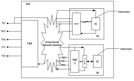
Consider a simple SoC that has 2 hierarchical components; Blocks- B1 & B2 as illustrated in Fig. 1. B1 has a WTAP interface while B2 has a JTAG interface. The SoC also has a top-level TAP, through which the 2 blocks are to be accessed. WTAP can easily provide the signals/bits from the core of B1 at its boundary, while the bits/signals associated with the core of B2 are brought at the boundary via TAP2 & TDR. However, to access these blocks from the SoC level, bits present at the respective block boundary have to be brought at the top-level. IJTAG P1687 provides a uniform access framework, communication protocol, and interface description required to define these bits at top-level. Furthermore, the IPs in SoC design need to communicate with one another as well. IEEE P1687 defines the scan path configurations between different IPs of the SoC and scan path configuration between the IP and the TAP controller that controls the communication among two IPs.

Fig. 1 Access WTAP/JTAG interface core from SoC TAP via unstructured network interface
Why is the JTAG/1500 standard not sufficient?
One may wonder whether the additional IJTAG network architecture is worth the cost of having extra hardware, which would increase the design area, especially when the embedded IPs can be accessed via JTAG TAP and TDR methodology. Here’s the answer; the purpose is to interface with the embedded MBIST instrument of B1. The instruction code fed into the IR selects the instrument to be interfaced. Thus, only one instrument can be accessed at once via single active IEEE 1149.1 instruction. The length of the TDR is fixed irrespective of the instrument selected on the chip. This means, the boundary scan chain length is fixed and has a fixed instruction configuration. Moreover, all the instruments would have to remain accessible throughout even if all of them are not targeted simultaneously since all are connected in a single-daisy chain [3]. The above-mentioned features make JTAG network inefficient with respect to Scan Path Management, which in turn leads to longer test time and ultimately higher test cost. IEEE P1687 standard has been proposed and formulated to overcome all of these limitations.
IJTAG use model
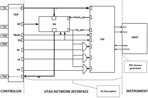
The IJTAG use-model shown in Fig. 2 explains the implementation of access methodology with the P1687 standard. It depicts three regions – the ‘Instrument zone’, which is targeted or which is to be interfaced with (rightmost region), the ‘IJTAG Network Interface zone’ present in the middle region, and the leftmost region is that of the ‘controller zone’ and comprises the TAP and its controller. It must be noted that the TAP controller, the 4 ports of the TAP, and the instrument are not a part of the IJTAG standard. In this model, the access of the instrument is done through the TAP just like in the previous scenario, however, the IJTAG network provides an interface platform that facilitates active scan path management thus providing a powerful plug and play feature to this standard.
The IJTAG use-model operates as follows:
- The ‘scan in’ (si) signal from TDI of TAP first enables the ‘select bit’ associated with the scan path of the instrument.
- This helps activate the specific scan path associated with the instrument which is to be interfaced with; in this case, the MBIST instrument
- This ‘select bit’ is referred to as Segment Interconnect Bit (SIB).
- The SIB generates the select signals locally that are fed to the TDR, which is responsible for access of MBIST instrument.
- MBIST controller begins the memory test once the ‘RUN’ signal is provided by the TDR. After the memory test is completed, the ‘DONE’ signal and ‘STATUS’ indicating PASS/FAIL status is fed back to the SIB via ‘from_so’ signal of TDR.
- SIB provides this PASS/FAIL signal to the TAP via the ‘so’ signal.
In this manner, the embedded MBIST instrument can be accessed via the top-level TAP in a SoC through the use of the IJTAG network interface.
Scan paths that enable access to the instrument under test can be closed after the instrument has been started [3]. For example, after all the start signals for the MBIST instrument are activated, testing of all the memory instances in complex SoCs would take a long time. Until the test is complete and produces PASS/FAIL status, the path would remain active if the SIB continues to be 1.

Fig. 2 IJTAG use model
This would unnecessarily keep the resources on this scan path busy and lead to longer test times. To prevent this, after all the instruments and TDR present on this scan path are made active, independent tests can be run offline and SIB control bit can be set to 0 again. This would allow the operations to start on other instruments and would not affect the instruments on inactive scan paths [3]. Launching simultaneous tests thus helps in reducing test access time. Furthermore, while we access a particular instrument, other instrument access is not required; the SIB associated with them can be disabled to keep it off the scan path. This too helps reduce access time, which is another significant benefit of this standard. The operation of the standard can be understood clearly once all the components of the IJTAG standard are described. This shall be covered in the next part of the article to be released soon.
Conclusion
In this part of the article, we examined how the fixed-length TDR and fixed instruction configuration of the JTAG standard make it inefficient to meet the growing demand of test design automation in a SoC with multiple embedded IPs. According to our brief description of the IJTAG use-model in this section, we looked at how test automation could be enabled using this standard. We also learnt that the IJTAG standard does not replace the existing IEEE 1149.1/1500 standard. Some of the leading vendors of the silicon industry are adopting this standard at a rapid pace as it provides ease of access to MBIST, internal scan chains of the chip, and in turn expedites debug features.
References:
- A Presentation Based on Slides Created by Members of the IEEE P1687 (IJTAG) Working Group, “IEEE P1687 (IJTAG) Draft Standard for Access and Control of Instrumentation Embedded Within a Semiconductor Device”, Jun 2006
- Laung-Terng Wang. Charles E. Stroud. Nur A. Touba, Laung-Terng Wang, “System-on-chip Test Architectures: Nanometer Design for Testability” Morgan Kaufmann Publishers, Version 2008.
- Al Crouch, “IEEE P1687 Internal JTAG (IJTAG) taps into embedded instrumentation” Asset White Paper, Version 2011
About Authors:
Medha Thakar
 Medha Thakar is working as an Engineer in the DFT BU, ASIC division, at eInfochips, an Arrow company. She has more than 1.5 years of experience in Design for Testing, which includes working on 16nm and 7nm technology nodes, handling block-level, and top-level DFT activities.
Chintan Panchal
 Chintan Panchal is working as a Delivery Manager in the ASIC division at eInfochips, an Arrow company. He has more than 18 years of experience in ASIC DFT. Over the years, he has worked on various technology nodes, from 180nm to 7nm, handling different DFT tasks, and managing a team of engineers.
