By Philippe Flatresse, Manuel Sellier (Dolphin Design)
1. The need for more and more edge processing capability
The Internet of Things (IoT) generates increasing amounts of data. According to IDC the number of connected devices will grow to 41.6 billion by 2025, generating 79.4 zettabytes (ZB) of data. Because of their variety and size these data need to be processed efficiently with new algorithms (cf. Figure 1). Neural networks processing has consequently become a key part of the value created by the emerging applications of the IoT world. Neural networks allow not only to treat extremely large sets of data, but also to extract key and invisible pieces of information.
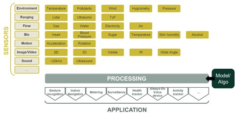
Figure 1: Sensor data processing is at the heart of IoT application innovation.
Neural networks’ data processing raises several challenges in terms of performance requirements. Therefore, the cloud was the first location to host this large processing demand, but this is currently evolving (Figure 2).
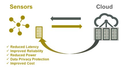
Figure 2: The need for more and more data processing closer to the sensors.
Firstly, connected devices often rely on a constrained power budget, limiting the capability to transmit large sets of data along wireless networks. Secondly, the connection between the end points and the cloud can have reliability issues, raising concerns about the reliability of the overall application. Thirdly, the inherent latency of the link between sensors and the cloud can have a bad impact at the application level. Finally, the data emitted out of the sensor raises inevitable privacy concerns.
For all these reasons, more and more computing capability is being transferred closer to the sensors, where the data is generated.
2. Limitations of current MCU solutions
Most often the first computing element through which sensors circulate data is the microcontroller unit (MCU). The MCU either gives feedback directly, based on the reading of the sensor and on certain instructions or – when the data is too complex to analyze – transmits the data for further processing in other computing elements, in the cloud for instance. Pushing more and more computing at the edge means transferring more and more computing capability to the MCU in order to take local decisions and action.
However, MCUs, as their name says, are good for control – not for processing. They are often based on architectures optimized for deep sleep mode, which can trigger efficient wake-up at every data event. The CPU is at the center of these centralized architectures and takes all decisions (Figure 3). These architectures make sense when the number of events is low, and when the processing required is relatively simple.
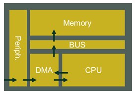
Figure 3: Standard CPU centric MCU architecture approach.
However, for processing large data flows – as is the case for artificial intelligence – MCUs often fail to meet the application requirements (Figure 4) and new architectures are required.
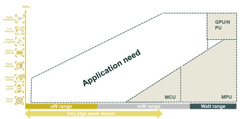
Figure 4: Limitations of standard computing architectures to enable a wide range of applications in the very edge power domain.
3. What needs to be changed
In order to implement efficient data processing solutions at the edge, MCU architectures need to be modified.
Firstly, an efficient fine-grained data power network needs to be implemented, optimizing not only leakage, but also dynamic power.
Then a new sensor-centric approach must be implemented, to avoid involving the CPU in all events in the case of large data collection. To do this, the data must be collected without involving the CPU. This can be performed using a modified subsystem architecture based on an autonomous DMA combined with an event manager. The CPU should also be able to compute the data without interfering with the data collection task. This can be done through a novel low latency interconnect, which minimizes data access conflicts.
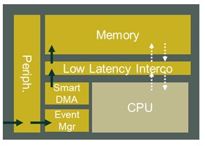
Figure 5: Innovative sensor-centric MCU architecture.
Finally, various specialized highly-efficient parallel computing blocks ranging from tiny Machine Learning (ML) to high performance neural network accelerators need to be added depending on the application requirement.
4. Dolphin Design SPEED MCU subsystem and computing platform offer
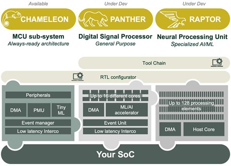
Figure 6: Dolphin Design MCU sub-system and processing platforms offers. Panther and Raptor platforms are still under development.
Dolphin Design has been working very intensively these last two years to develop three new System Platforms for Energy Efficient Design (SPEED), which integrate all the good practices mentioned above.
- ·Chameleon
- Chameleon is a configurable MCU sub-system embedding several standard peripherals, an autonomous DMA, a fined-grained power management unit, a tiny ML accelerator, a low latency interconnect, and an event manager. All these features provide extremely low power consumption in both deep sleep and active modes.
- The platform comes with an RTL configurator tool and all necessary drivers.
- ·Panther – under development
- Panther is a highly configurable DSP platform based on up to 16 processing elements and an ML/AI accelerator. The platform embeds an event manager as well as a low latency interconnect to maximize the energy efficiency.
- The platform will come with an RTL configurator and a tool chain.
- Panther will enable more than 7GOPS computing performance and an efficiency of 120GOPS/W (@2.2GOPS) in 40 nm LP technology.
- ·Raptor – under development
- Raptor is a Neural Processing Unit specialized in vision processing algorithms, which includes a host core, a DMA, and up to 128 processing elements.
- Raptor will enable more than 60GOPS computing performance and an efficiency of 2200GOPS/W (@16GOPS) in 28 nm FD-SOI technology.
5. Benchmarks
As depicted in Figure 7 we see clear benefits to using Dolphin Design SPEED platforms compared to standard MCU platforms. Highly energy efficient solutions can be designed in the very edge power range, enabling a wide range of new applications.
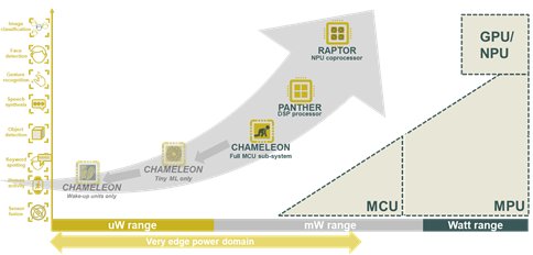
Figure 7: Dolphin Design SPEED MCU sub-system & processing platform benchmarks in 40LP.
6. Example of audio applications
Audio or Always-On Voice (AOV) devices are perhaps one of the most thrilling applications, which can take advantage of Dolphin Design’s new SPEED MCU sub-system and processing platforms.
An AOV device is a voice-controlled device, listening 100% of the time in order to recognize keywords in the sound environment. Many analysts, such as Duncan Stewart from Deloitte, think voice interface will become the de facto interface in the near future for increasing amounts of home appliance devices.
Several start-ups have emerged to enable this new kind of interface. However, they often propose only a closed hardware solution in the form of an AOV interface chip, or a full MCU chip. By combining Dolphin Design’s audio platform (called Bat) and the Chameleon MCU sub-system, any SoC designer can embed a very efficient sub-150 µW voice interface in his project, without having to rely on a closed hardware solution as illustrated below.
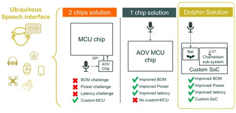
Figure 8: Current solutions to enable efficient Always-On Voice devices.
7. Take-away
The edge processing revolution is about to change the MCU market. More and more companies will need to boost the processing performance of their MCU solutions. This will require the adoption of new sensor-centric MCU architectures (sub-systems and accelerators), which are less dependent on the CPU and more autonomous, to collect and treat the data flow in a very efficient way.
Dolphin Design has been working intensively to offer three new MCU sub-system and computing platforms compatible with a sensor-centric approach. These platforms offer substantial energy efficiency gains for a wide range of edge computing projects.
The availability of such platforms will ease the SoC designer’s life while inventing new applications with significantly more intelligence at the edge.
ABOUT THE AUTHORS
 | Philippe Flatresse received PhD degree in Microlectronics in 1999 from the Institut National Polytechnique de Grenoble. During his thesis, he has developed the LETISOI spice model dedicated to SOI technologies at CEA LETI. In year 2000, he joined STMicroelectronics Central R&D to deploy the SOI digital design activity. He has pioneered the partially and fully depleted SOI technologies and demonstrated their key advantages for low power high performance digital applications. As design architect, he contributed to the development of products targeting high-growth areas such as ADAS, MCU and IoT applications. He was in charge of exploring the energy efficiency limits on multi-cores systems for ultra-low power processing by combining FD-SOI technology with body biasing, advanced low power techniques. In 2017, he joined SOITEC as expert for digital applications to participate to the worldwide promotion of SOI technologies. He is now director of business development and marketing team at Dolphin Design. |
 | Manuel Sellier is Soitec’s product marketing senior manager, responsible for defining the business plans, marketing strategies, and design specifications for various energy efficient product lines including the fully depleted silicon-on-insulator (FD-SOI) technology. He is currently supporting Dolphin Design in the deployment of their new SPEED platforms (System Platforms for Energy Efficient Design). Before joining Soitec, he worked for STMicroelectronics, initially as a digital designer covering advanced signoff solutions for high-performance application processors. He earned his Ph.D. degree in the modeling and circuit simulation of advanced metal–oxide–semiconductor transistors (FD-SOI and fin field-effect transistors). He holds several patents in various fields of engineering and has published a wide variety of papers in journals and at international conferences. |
