By Sarita Yadav, eInfochips - An arrow company
As technology advance, we see complex SoCs emerging in the market with multiple interfaces. These complex SoCs can have multiple clocks driving multiple modules, which may be getting divided further to generate new clocks in the chip and so the complexity increases.
Dynamic clock switching means that the clock frequency changes anytime during simulation, even in the middle of ongoing transactions. Most of the time, to verify a device under test (DUT), we prepare a testplan and all features are verified by generating stimulus, developing test cases, and comparing with scoreboard, checkers, predictor models, assertions, and coverage. Along with other features, one of the very important factors to consider during verification is the clocks. We perform register testing to ensure all registers in DUT gets updated as expected, which covers clock registers as well. But the clock register updating correctly doesn’t ensure that the desired clock changes have happened. Many a time, we miss verifying the clocks thoroughly which results in issues at a later stage of chip tape-out.
In cases where clock frequency changes on-the-fly, which means clock speed can be varied through register programming, the clock verification becomes even more crucial for the chip to be a success. During frequency switching, the clock may have a glitch, which usually is very difficult to catch, until we have a proper checking mechanism in place to verify clocks.
The data integrity can be checked by the testbench components like a scoreboard, and predictors but none of the testbench components checks the correctness of clocks, whether the frequency switching has happened or not, and if there are any glitches in the clock generation. Along with data integrity, we need to ensure that clock frequency has changed as expected and is glitch-free.
This paper will describe an approach to verify dynamic clock switching.
Scenario
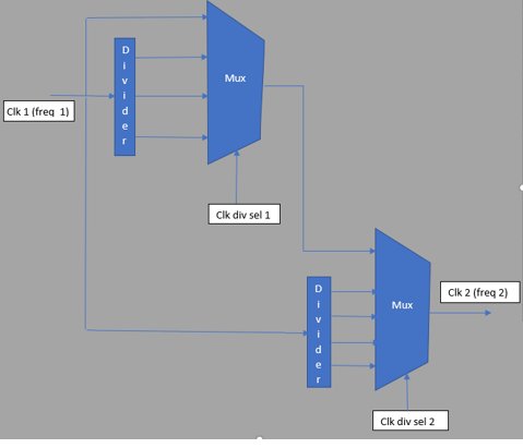
Figure 1 below shows an example of a clock generation based on clock divider register values. clk_div_sel1 and clk_div_sel2 are the register bits and are used to generate different clock frequencies. These registers can be written at any time during simulation to switch the clock frequency dynamically.

Figure 1: Clock divider
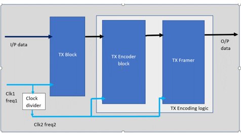
Figure 2 below shows how the clock divider shown in figure 1 is used inside DUT to generate clocks and drive them to different modules.

Figure 2: DUT having different blocks with different clocks
Let’s assume a scenario where we write to clock registers and the clock frequency is expected to change on-the-fly from frequency 1 to frequency 2 and then to frequency 3 in the middle of ongoing traffic. The clock frequency change in the middle of the transaction may cause loss of data or may cause the modules to get stuck if there is any handshaking between the modules. We need to ensure 3 things here –
- Register gets written correctly
- Data integrity is maintained, there is no loss of data
- Clock frequency switching happens as expected
We can write and read back the register and ensure that the register got written correctly. The scoreboard in our testbench will check for data integrity. These checks we generally perform in any testbenches. Our testplan usually have register testing and data integrity with various possible stimulus. Points 1 and 2 mentioned above are most likely to be verified and covered in any verification. The crucial part is to check whether the clock is generated as expected.
Now, what if even after writing to the register, the register gets written, and when we read back we get the updated value as expected but, the clock is still running at an old frequency (say, freq 1). There may be other scenarios where the clock has changed to freq 4, instead of freq 2 or 3 or, when the clock frequency has changed to freq 2 as expected but there can be a glitch while switching frequency. Even with glitches, the data is correctly passed on to the output interface with the scoreboard showing data match. Is the verification done? The answer is No!!
Solution
The solution is to have a clock checker module, which keeps checking the frequency and shouts an error if there is any glitch or the frequency switching isn’t as expected. There can be multiple ways to write a clock checker module, but system Verilog provides a powerful subset, which is assertions that can be used in the clock checker module. Assertions are very powerful if written correctly and efficiently. Assertions are an efficient way to not only check the clock frequencies but also to catch issues if there is any glitch in the clock while switching frequency, which is difficult to catch otherwise.
Look at the figure below showing clock frequency change with a glitch while switching frequency. 
The issue shown in the above figure can be easy to catch with the clock checker module. The assertion will fail as and when the frequency is not as expected or if there is any glitch in the clock.

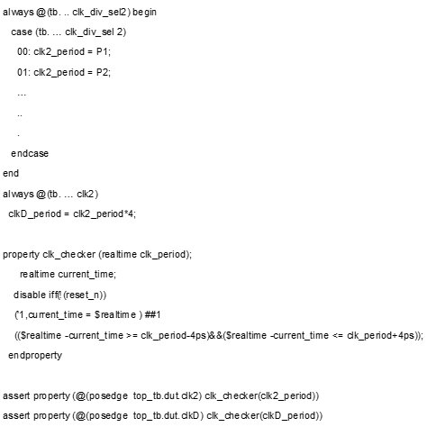
In the scenario mentioned above, the clock is switching multiple times on-the-fly in the middle of the simulation. This clock may be driving multiple modules or it may be divided further to drive other modules in the design. The clock checker module predicts the expected frequency of all the clocks in the design by looking at the register configuration and check the clock frequency against the predicted/expected frequency. Now, in a design, there may be multiple clocks that may be getting divided further resulting in N number of clocks to be verified. To achieve this a generic property can be written to which the clock period is the input parameter and assertions can be written for this property passing the clock period. The property is generic, and this piece of code can be re-used to check multiple clocks in the chip. This approach ensures optimization of the code as the same assertion property will be used to verify all the clocks in the DUT.
Code Example

When registers are configured to switch the clock, clk2_period is calculated based on the register programming of clk_div_sel 1 and clk_div_sel 2. This serves as the expected clock frequency for the clock checker. When the clock changes on-the-fly, the clock module has the expected clock period and it keeps verifying clock frequency against it and the assertion will fail if the clock isn’t running at an expected frequency or if there is any glitch occurred during frequency switching. The same property can be called for all the clocks in the design. The assertions used in the clock checker module should be part of our testplan and coverage. The assertion coverage will ensure that all clocks are verified.
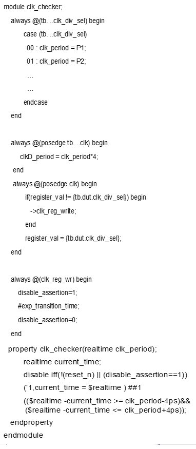
The above solution was considering that the design expects no glitches during clock switching. There may be cases where the clock switching in the design is not smooth and the design may expect some glitches during the transition period. The transition period may be short enough or maybe a little longer to get settled to its final frequency. And since these glitches are expected, our assertion should not shout out any error during that transition time. The design specification tells us the transition period the design expects. Based on that we can disable our assertion during that transition window. Another possible scenario could be where writing to divider register and the actual clock switching has some expected switching window. In either case, during verification, we can consider a near to exact transition window during which assertion will be disabled. If there are any glitches after the clock gets settled, will be caught by the assertion.
Code Example considering design expectation

In the code example above, whenever there is a clock divider register value change, an event is triggered which in turn sets disable_assertion control variable to 1. After the expected transition window, which we get from design spec, we make disable_assertion to 0. The assertion will be disabled when disable_assertion is 1. This way the verification ensures accurate and complete clock verification for both the scenarios where the clock switching is expected to be completely smooth and where glitches are expected and ok to have in RTL.
So, we can verify clock frequencies, dynamic frequency switching, and correctness of clock by modeling a clock module using assertions.
Conclusion
Clock verification is very crucial in verification and must be carried out thoroughly. Based on the specification and register configuration, the clocks can be verified by determining the expected clock frequency, which can then be used in the clock module to verify all the clocks. To avoid having code written for individual clocks, a generic code can be written which can be re-used for all the clocks and across testbenches to verify the clocks. This is how we can verify all the clocks in the DUT.
For more information, please free to connect with our experts today.
About the author
Sarita Yadav works in ASIC BU of eInfochips- An arrow company. She has experience in ASIC verification, functional verification, and the development of SOCs in various domains like networking and communication. She worked on advanced methodologies like UVM, System Verilog, Assertion, coverage-driven verification, eRM, specimen, etc.
