By Hai YU, Clément MOULIN (Dolphin Design)
In this second part of Paving the way for the next generation audio codec for True Wireless Stereo (TWS) applications whitepaper, energy efficiency will be discussed and several means to achieve extra-long playtime will be exposed.
Figure 1 highlights the functions under discussion amongst the main functionalities embedded in earbuds.
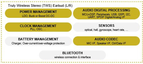
Fig.1: Functional blocks of a typical TWS earbud chip
1- About power consumption
When thinking about TWS audio systems in daily use, there are several ways to enhance the customer experience and provide a hassle-free user interface integration. One of the critical issues TWS system designers are facing is playtime, because battery space is usually very limited in TWS earbuds. In a TWS system, the tiny battery constrains the power and energy available for the entire system, which comes at an extreme premium in TWS earbuds, where only the tiniest battery fits. For example, the Apple Airpod earbud has a 93 mW-hr battery, which is roughly only 1% of the battery capacity of an iPhone 7. Light and handy is the most important design goal of TWS headsets. Limited by the small space of the charging cradle and the headset, the battery capacity used in these two parts cannot be increased. The capacity of the charging cradle is generally less than 1000 mAh (commonly in the 200-700mAh range), and the capacity of the headset is smaller, mostly less than 100 mAh. Therefore, whether it is a charging cradle, an earbud or a headset, attention should be paid to the low-power design of the system to ensure that the TWS product has a longer battery lifetime.
Like other IoT systems that are based on battery, power consumption remains one of the challenging topics in TWS systems. The main power consumers are the PMIC or integrated PMU, the digital audio processing chain, noise suppression software, and other audio signal processing algorithms executed on MCU or DSP, etc. To achieve the best noise resilience efficiency in a TWS system, a large amount of data processing capability (with limited hardware resource) is required (ambient noise cancellation, keyword spotting, hybrid ANC, acoustic echo cancellation, dynamic range compression, and even for multi-microphone beamforming and position-aware applications), which may cause over-consumption issues. Consequently, both audio data processing and power consumption should be taken into consideration during the TWS system design, to achieve the best trade-offs. If the power consumption in TWS earbuds or headphones is not well addressed, it will not only shorten the battery lifetime, but it might cause heating, hearing and comfort problems. Therefore, low power consumption is an important factor for TWS earbuds and headphones design.
The power consumption of the audio codec itself might not be the most power consuming element in the whole audio signal processing chain but it is not negligible either. There are three power consumption optimization aspects that can be considered in the audio signal chain.

Fig.2: Overview of audio signal chain in TWS IC
First and foremost, the Voice Activity Detection (VAD or wake-up word) add-on feature. An Always-On Voice (AOV) device is a voice-controlled hardware device, listening 100% of the time to recognize keywords in the sound environment, consuming only a fraction of the power that a software algorithm and/or conventional DSP would require. To minimize the overall power consumption, an AOV device can be used to wake up the system, allowing unused elements of the audio signal processing chain to be turned off during listening mode (ADC channels, DSP and/or MCU, digital filters, etc.).
| Dolphin Design WhisperTrigger: Voice Activity Detector (VAD) WhisperTrigger is Dolphin’s state-of-the-art Voice Activity Detector (VAD) which detects the presence of voice in a sound, and triggers a system wake-up interrupt signal. The analog and digital solutions for VAD are called WT-a and WT-d respectively. The microphone technology (analog or digital) will drive the choice between these two solutions. To minimize power consumption, the VAD IP must be integrated between the microphone and the ADC for WT-a, and between the microphone and the decimation filters for WT-d, This solution has the undeniable advantage of being able to operate without any DSP resources. |
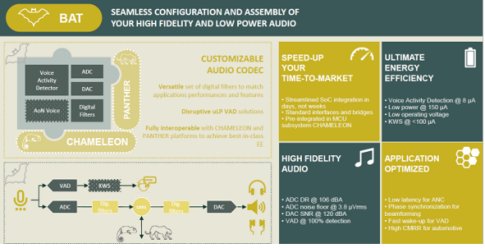
WhisperTrigger is part of Dolphin’s BAT audio platform, enabling a seamless configuration and assembly of your high fidelity and low-power audio device (always-listening TWS earbuds/headsets, or always-listening TWS smart speaker), offering the best analog performances with high configurability of digital filtering. Dolphin’s highly customizable and patented VAD solution offers on-the-fly customization capabilities that allow you to adapt to any kind of environment. It can adjust automatically according to the ambient noise with the lowest detection latency and best Voice-Detected-as-Voice / Noise-Detected-as-Voice (NDV) trade-off, and it also constantly detects the ambient noise floor level (NFI signal) which can be used by the downstream audio signal processing engine for an optimal adaption of the keyword spotting algorithm in accordance with the environmental conditions.
Fig. 3: Overview of high performance highly configurable BAT platform
Secondly, various operating modes are supported in case of multiple ADC/DAC channels, such as TWS earbuds (for example, 3 microphones per ear). When the ADC or DAC is not required to run in full performance mode, the corresponding ADC/DAC channels can be set to low-power or ultra-low-power mode to minimize power consumption.
| Dolphin Design ADC ultra-low power mode In Dolphin Design’s ultra-low power ADC, each channel works independently and can be configured in different operating modes to face different application scenario requirements. In TSMC 22 nm uLL process technology, the mono ADC consumes only 150 µA (compared to 600 µA in normal operating mode), which allows to optimize further the power consumption. |
Last, but never least, the ultra-low latency I/O digital filters of our audio codec can assist in power consumption optimization. With less I/O digital filter latency, the ANC algorithms can achieve the best noise-cancellation performance, and optimize design margin and signal processing hardware resources, thus reaching closer to the ultimate power optimization.
2- High configurability and high flexibility
Having the most frugal IPs is not sufficient if they are not tailored to the application to be sure no supplementary unused hardware is present in the chip. This section focuses mainly on the configurability and flexibility of Dolphin Design’s state-of-the-art audio codec IP which can be configured and optimized for different audio application requirements.
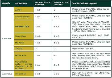
For TWS earbud applications with a hybrid ANC feature, depending on the digital or analog MEMS type, it requires 3 microphone interfaces to pick up the audio stream from the 3 microphones (one for FF, one for FB and one for phone call). To provide full flexibility to the client, Dolphin Design’s audio codec IP supports stereo to eight digital microphone interfaces (pulse-density-modulated or PDM inputs), and mono to eight ADC channels for which each channel can be operated in an independent manner, which makes it possible to reduce the power consumption under certain application usage scenarios. The audio playback path supports from mono to eight DAC channels. The channel number of the digital microphone interface, ADC recording path and DAC playback path is configurable. This means that, depending on the targeted audio application requirements, the audio codec IP is fully configurable with its basic internal blocks fully silicon-proven (available both for Global Foundry 22 nm FD-SOI and TSMC 22 nm uLL process technologies).
In addition, as stated in the previous section, the audio sampling frequency (Fs) is highly configurable to adapt to the various application requirements. The dedicated digital filters of the TWS system are specially designed to support an audio sampling frequency from 16 kHz to 768 kHz to achieve the ultra-low input-to-output (or analog-to-analog) latency. Finally, Dolphin Design’s audio codec IP supports both master mode and synchronous slave mode, which provide flexibility to the end customer for different application usage scenarios without any performance degradation.
The Audio Interface Adaptive Synchronizer (AIAS) is embedded inside Dolphin’s audio codec IP. The AIAS functionality is based on the continuous measurement of the I2S interface sampling frequency (word clock frequency). It locks and tracks the sampling frequency, then drives the digital audio filtering chain to make it work at the measured sampling frequency without any performance drop, and the system continuously follows the sampling frequency variation and compensates the input clock jitters. In short, the AIAS feature is specially designed for:
-
automatic detection of the sampling frequency (Fs) without any settings when audio codec works in slave mode.
-
interfacing the different clock domains (up to +/- 3% error tolerance) that make the audio codec, with higher resilience both to master clock jitters and serial data interface clock jitters.
-
supporting and tolerating the sampling frequency variations to synchronize different video and audio streams.
3- Managing power efficiency
Achieving long play time is impossible if the power supply efficiency does not receive the same level of care and optimization as the audio process. In this following section a quick overview of the key parameters and Dolphin’s Design proposal will be discussed.
In TWS chip/SoC design, the most important component is of course the Li-Ion Battery and a charger to enable charging the cradle’s battery with a standard USB 5V supply. Power management blocks like LDOs and DC/DC converters distribute required supply voltages to the various voltage domains. A dedicated 5V supply is mandatory to provide power for the earbuds to charge their batteries, which forces the TWS IC design teams to pursue tough power objectives: zero power consumption in stand-by mode, and maximum performance in operational mode with optimized energy efficiency. Energy efficiency is the key metric which demonstrates the maximum that can be done with the minimum energy.
Voltage regulators are basically split into two categories: linear regulators (LDO) and switching regulators (DC-DC converters). Selection depends on application constraints and is often a smart trade-off between power efficiency, silicon area and BoM costs.
Leakage current is one of the key analog characteristics that must meet the tight power constraints of the TWS systems, but the capability of a DC-DC converter to demonstrate high efficiency, whatever the output current, is a real challenge for analog designers that want to maximize battery autonomy. When it comes to achieving ultra-low power figures in sleep and active modes, then the challenge moves from high efficiency to low quiescent current, which can generally be achieved using low-quiescent LDOs to supply the Always-On domain.
PMU control is also a keystone of the power management strategy. It drives the boot-up sequence, configures the voltage regulators to get the correct output voltage for a given power mode, and ensures that power sequencing is properly executed. There are currently two ways to implement a PMU: full custom design or software PMU.
A full custom PMU can achieve ultra-low power figures, especially if it is implemented with low leakage logic cells in the Always-On domain, however it suffers from a lack of configurability and needs to be fully re-designed if there is a change in the SoC architecture or for a product derivative.
A software-based PMU relies on an embedded core, typically a small MCU block, to control power mode sequencing and to manage the interrupts. It can easily be re-configured in-field using conventional firmware updates, however the need to have an MCU that is always active (to control the SoC activity) makes it incompatible with dormant applications that require ultra-low power consumption in hibernation mode.
| Dolphin Design SPIDER platform: turnkey solution to accelerate the design of advanced power management solutions Dolphin Design brings the most advanced solution to secure the silicon and keep the time-to-market under control, with its combination of a state-of-the-art power management IP portfolio (low-leakage LDO, nano-power high-efficiency DC-DC), a fully configurable and low-power Power Controller IP (MAESTRO) scalable to any SoC complexity, and the unique PowerStudio system tool that speeds up power architecture exploration and PMU seamless integration. |
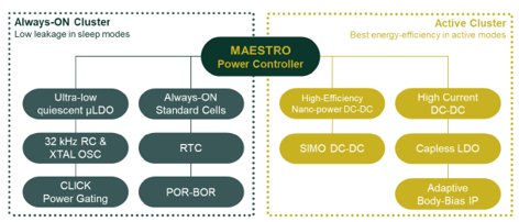
The MAESTRO Power Controller brings you ultra-low consumption and high-flexibility for a best-in-class energy efficient power network. Built on a CPU-less architecture scalable to any SoC complexity, it manages the way energy is distributed to each block in the circuit, controls power sequencing and ensures that retention, power gating and isolation strategies are under control. MAESTRO works hand-in-hand with our power management IPs and is seamlessly configured with PowerStudio for a fast and predictable integration into your SoC:
- Scalable to any SoC complexity
- Fast and easy configuration with PowerStudio
- CPU-less and event-based architecture for ultra-low power consumption
Fig. 4: Overview of Maestro Power Controller
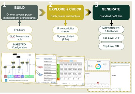
PowerStudio profits from Dolphin Design’s long expertise with power management design optimization. Compatible with any process node, already pre-configured with our IP portfolio and open to 3rd party IPs, it provides you with a single cockpit to build a safe power network configuration that matches your application requirements. From early power architecture exploration up to RTL/UPF low-power flow enablement, PowerStudio is at your side to standardize and accelerate your power management design flow.
- Fast power architecture exploration and selection.
- Smooth MAESTRO power controller configuration with automated test bench generation.
- Automated generation of RTL and UPF files to bridge the gap with front-end design flow.
- Open to third-party IPs and ready to support any process node.
Fig.5: Overview of Power Studio Software and Design
ABOUT THE AUTHORS
Hai YU received his PhD in Nano and Micro Electrical Engineering in 2011 from TIMA laboratory, Grenoble Alpes University for his work on low-cost highly efficient fault tolerant processor design for mitigating the reliability issues in nanometric technologies. Hai joined Dolphin Design in 2012 and is currently working as a Lead Application Engineer, focusing on Audio & Processing IPs platforms.
Clément MOULIN graduated from ENSEEIHT Toulouse in electronic and signal processing in 2006. After 8 years of leading hardware development in NFC domain, Clément joined Dolphin Design in 2020 and is currently working as an Application Engineer, focusing on Audio & Processing IPs platforms.

