By Thevin Arokiaraj L, Nikila S (HCL Technologies)
1- Abstract
Most of the modern SoC’s have one or more low power features. While the SoC’s that go into battery operated end products have aggressive low power features, other SoC’s still have some basic low power features. The goal of low power design is to reduce the power consumption of individual IPs (Intellectual Property) . This can be achieved by incorporating low power design strategies and rules in the SoC.
This paper discusses about the low power IP components from ARM can help one to realize the low power features in the SoC. It should be noted that this paper does not discuss about the low power concepts or design techniques. Rather, it focuses on the implementation approaches using ARM low power IP.
Keywords: Low Power, Power Gating, Power Consumption, SoC Design, VLSI, Intellectual Property, SCP, Power Policy Unit
2- Glossary
| Abbreviation | Description |
| ADB | Access Domain Bridge |
| AI | Artificial Intelligence |
| AON | Always On Domain |
| APB | Advanced Peripheral Bus |
| AVFS | Adaptive Voltage and Frequency Scaling |
| AXI | Advanced eXtensible Interface |
| CLK-CTRL | Clock Controller |
| CPU | Central Processing Unit |
| DMA | Direct Memory Access |
| DVFS | Dynamic Voltage and Frequency Scaling |
| FSM | Finite State Machine |
| GPIO | General Purpose Input/Output |
| I2C | Inter-Integrated Circuit |
| IB | Interconnect Bus |
| IP | Intellectual Property |
| LP | Low Power |
| LPC | Low Power Combiner |
| LPD | Low Power Distributor |
| LSP | Low Speed Peripherals |
| PCM | Power Control Module |
| PCSM | Power Control State Machine |
| PD | Power Domain |
| PDCM | Power Dependency Control Matrix |
| PPU | Power Policy Unit |
| RAM | Random Access Memory |
| SCP | System Control Processor |
| SoC | System on Chip |
| SPI | Serial Peripheral Interface |
| UART | Universal Asynchronous Receiver-Transmitter |
3- Introduction
A typical System on Chip (SoC) consists of a CPU, a memory interface, peripheral interfaces, and other application specific IP’s (e.g. MIPI CSI-2 for camera sensor interface). Hence, Low power design has to be implemented for efficient power supply to the SoC without any major compromise in performance and scalability. Some commonly used techniques used for low power design implemented in this SoC design that aim to reduce static and dynamic power consumption are:
- Clock Gating
- Power Gating
- Logic and Memory Retention with Power Gating
In this paper, we will first review the low power techniques, then we will look at the low power design architecture for SoC design and after that we will focus our discussion on the implementation of the LP (Low Power) design using LP interconnect and power controller components. The low power interconnects and controller components discussed in this paper are Arm© owned Intellectual Properties(IPs). Power Control State Machine (PCSM), however, is a custom design logic and is intimately tied to a specific Sub-system’s low power features to be supported.
Section 4 has the basic description of Low Power Design Techniques and how the aforementioned techniques are implemented using various Low Power components. Section 5 captures information on Low Power IP components that provide the desired power gating to SoC. Section 6 describes how the Low Power Components are used in SoC Design followed by conclusion in Section 7.
4- Low Power Design Techniques
There are many low power design techniques that are used in the contemporary designs. The techniques are:
- Clock Gating
- Multi-Voltage
- Power Gating
- Retention with Power Gating
- Advanced techniques such as DVFS (Dynamic Voltage and Frequency Scaling), AVFS (Adaptive Voltage and Frequency Scaling), well biasing and usage of specialized low power library cells.
However, this paper uses only the following techniques, as the focus of this paper is on implementing the low power design using ARM’s IP rather than the low power design techniques itself:
- Clock Gating to reduce dynamic power
- Power Gating in the SoC design to reduce leakage power
4.1- Clock gating
This technique is the most widely-used method for implementation of low power design and is also well-supported in many tool flows. The ultimate goal of implementing this technique is to reduce dynamic power. Clock gating is a very simple technique to reduce power and area by using the clock enable signal to perform clock gating thereby to reduce the capacitive load and activity factors which reduces the switching power component of dynamic power.
4.2- Power gating
In power gating technique, the power supply to each power domains are controlled by power switches that can be turned ON or OFF. The ON and OFF conditions of the power switch is itself dependent on the power state of a given subsystem, which is highly application specific. Power gating typically involves shutting off a power domain completely thereby resulting in saving of both static and dynamic power. In most cases, when a sub-system is powered down, it is necessary to make sure that its output voltage levels are clamped. This ensures that the sub-system holds benign values at its output when it is powered down. This is achieved by using “Isolation cells” that clamps the inputs/outputs of a power domain to a known value during OFF state. A power management unit that controls the power switch and isolation enable signals must be implemented such that these signal values during shutdown are clamped to the right values.
5 Low Power IP Controller Components used in SoC Design
The design components explained in this section are essential for implementing the low power features in an ARM based SoC.
5.1 Power Policy Unit(PPU)
Power Policy Unit (PPU) is used to provide power domain control in every subsystem in an SoC. PPU contains the following interfaces:
- Software Interface: For providing power policy control and component configuration.
- Clock control Interface: For clock gating interface.
- Device Control Interface: For providing power transition request and ensuring device quiescence.
- Device Interface: Consists of one or more Low Power Interface P/Q-channels.
- Control Interface: Clock enable, resets and Isolation enable signals.
- Power Control State Machine Interface: For providing power switch and retention control.
PPU provides hardware and software interfaces for controlling the various power modes that are defined for the SoC to effectively manipulate device quiescence for optimal power consumption. The PPU device interface uses either one P-Channel or Q-Channel to interface with the IP component for handling device quiescence. Some of the IP component doesn’t provide P/Q-channel support. In that case, PPU device Q-channel can also be interfaced with an ADB (ARM’s Access Domain Bridge IP) slave Q-channel that handles the power state transition request from PPU. If the IP component is performing any transactions to other IP component through ADB, then ADB will send the deny response to PPU to avoid any fly off transactions during power down.
PPU uses power modes such as ON, OFF and RETENTION to represent various combinations of logic and memory power states of a domain that can be specified. Below block diagram shows the connectivity of PPU with an IP component with PCSM performing power switch control transitions:
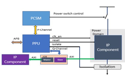
Figure 1: Power Policy Unit
5.2 Power Control State Machine(PCSM)
PCSM is a simple state machine to perform Power and Retention Controls. PPU and PCSM are interfaced through P-Channel interface, without PDENY or PACTIVE. The following are the four output Power control signals:
- lgcpwrn – Active LOW control signal for logic power signal.
- lgcretn – Active LOW control signal for the logic retention power signal.
- rampwrn – Active LOW control signal for the RAM power signal.
- ramretn – Active LOW control signal for the RAM retention power signal.
Each PPU has a P-Channel interface that connects to a Power Control State Machine (PCSM). The following figure shows the PCSM P-Channel handshake waveform.

Figure 2: PCSM P-Channel Handshake Waveform
When the power modes changes happen, PCSMPREQ signal will be set high by the PPU. PPU directs the PCSM to do the power control and retention transitions by changing the modes in the PCSMPSTATE input signal. Based on the power modes changes by the PPU, PCSM will change the values of four output Power Switch Control signals. The P-Channel interface remains in PCSMPREQ until all the power control switches and the respective delays are applied. Only after this, the PCSMPREQ is pulled LOW when the request is accepted by the assertion of PCSMACCEPT and the handshake is considered to be complete.
The PCSM responds to requests on the P-Channel, to change the values of the power control switches as required. Each transition, on the P-Channel, converts into several PCSM transitions. The following table lists the transitions for the logic power mode changes.
| Logic Transition Name | lgcpwrn | lgcretn | Delay Applied | Description |
|---|---|---|---|---|
| LGC_ON | 0 | 1 | LGC_OFF_ON_DLY | Logic power switch is turned on. |
| LGC_OFF | 1 | 1 | LGC_ON_OFF_DLY | Logic power switch is turned off, when moving to off. |
| LGC_ON_ONRET | 0 | 0 | LGC_ON_ONRET_DLY | Logic retention switch is turned on. |
| LGC_ONRET_RET | 1 | 0 | LGC_ONRET_RET_DLY | Logic retention switch is turned off when moving to retention |
| LGC_RET_ONRET | 0 | 0 | LGC_RET_ONRET_DLY | Logic power switch is turned on, when moving to on from retention. |
| LGC_ONRET_ON | 0 | 1 | LGC_ONRET_ON_DLY | Logic retention switch is turned off, when moving to On. |
Table 1: Logic Transitions
The following table lists the transitions for RAM power mode changes.
| RAM Transition Name | rampwrn | ramretn | Delay Applied | Description |
|---|---|---|---|---|
| RAM_ON | 0 | 1 | RAM_OFF_ON_DLY | RAM power switch is turned on. |
| RAM_OFF | 1 | 1 | RAM_ON_OFF_DLY | RAM power switch is turned off, when moving to off |
| RAM_ON_ONRET | 0 | 0 | RAM _ON_ONRET_DLY | RAM retention switch is turned on. |
| RAM_ONRET_RET | 1 | 0 | RAM _ONRET_RET_DLY | RAM power switch is turned off, when moving to retention. |
| RAM_RET_ONRET | 0 | 0 | RAM _RET_ONRET_DLY | RAM power switch is turned on, when moving to on from retention. |
| RAM_ONRET_ON | 0 | 1 | RAM _ONRET_ON_DLY | RAM retention switch is turned off, when moving to on. |
Table 2: RAM Transitions
The sequence of the RAM transition and logic transition depends on the current power mode and the requested power mode. The following table lists the possible combinations:
| Current Power Mode | Requested Power Mode | PCSM Sequence |
|---|---|---|
| OFF | OFF | No Transition Required (P-Channel handshake completes) |
| ON | 1. LGC_ON 2. RAM_ON | |
| FULL_RET | FULL_RET | No Transition Required (P-Channel handshake completes) |
| ON | 1. LGC_RET_ONRET 2. LGC_ONRET_ON 3. RAM_RET_ONRET 4. RAM_ONRET_ON | |
| MEM_RET | MEM_RET | No Transition Required (P-Channel handshake completes) |
| ON | 1. LGC_ON 2. RAM_RET_ONRET 3. RAM_ONRET_ON | |
| ON | OFF | 1. RAM_OFF 2. LGC_OFF |
| FULL_RET | 1.RAM_ON_ONRET 2.RAM_ONRET_RET 3. LGC_ON_ONRET 4. LGC_ONRET_RET | |
| MEM_RET | 1. RAM_ON_ONRET 2. RAM_ONRET_RET 3. LGC_OFF | |
| ON | No Transition Required (P-Channel handshake completes) |
Table 3: Power Mode Transitions
Consider an example when the current power mode is OFF and the requested power mode by the PPU is ON, PCSM does the LGC_ON and RAM_ON power mode transitions in the sequence. The following figure shows a diagrammatic representation of the PCSM power mode transitions.

Figure 3: PCSM Power Mode Transitions Sequence
5.3 Low Power Distributor (LPD)
Low Power Distributor (LPD) are used to distribute one low power controller interface signals to multiple low-power channel compatible-device component interfaces. This component can be operated in two modes: Expander mode or Sequencer mode. In Expander mode, power state transition request from a power controller is simultaneously sent to all device components. Response of acceptance or denial for entry to a low power state can be received by the distributor in no particular order whereas in Sequencer mode, request from power controller to a low power state will be sent to the last device in the chain and a response is expected before the request is sent to another device component. However, this distributor can only be used when the device components exist in the same power domain.

Figure 4 Low Power Distributor
5.4 Low Power Combiner Q-channel(LPC-Q)
This low power component has the ability to control one or multiple device components by two or greater number of power control components that have the same control interface requirements. Essentially, this component is used to provide N:1 fan-in from controllers to a component. However, this component is majorly used there is a cross-domain component such as an Access Domain Bridge(ADB) that must be put to a low power state before either of the associated components’ power domains switch off or put into retention.

Figure 5: Low Power Combiner
5.5 Clock Controller (CLK-CTRL)
Clock-controller is essentially used to provide clock-gating for devices via the Q-channel interface when they are transitioned to OFF power state. One advantage of using the CLK-CTRL rather than a generic clock gating technique is that this component ensures that a device is non-functional or in a low power state before gating the clock so as not to affect the functionality of the device. It also ensures that the clock is being supplied to the device, before the device exits the low power state.
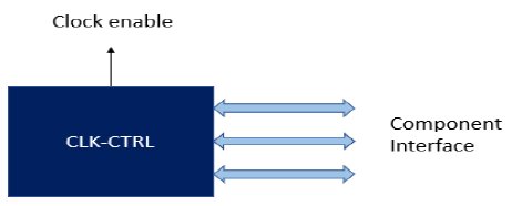
Figure 6: Clock Controller
6 Low Power Design Architecture
6.1 Top-Level SoC Design Hierarchy
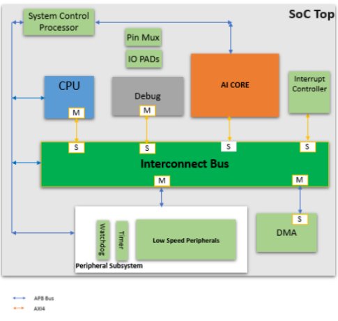
Figure 7: SoC Block Diagram
This particular implementation of SoC contains CPU having Instruction and Data Cache for each Core and also has internal boot memory support. AI core is a scalable and highly configurable architecture model that is used to design Deep Learning Accelerators with attached SRAM memory and AXI memory controller for register access configuration. Interrupt Controller that performs critical tasks of interrupt management, prioritization and routing. Low Speed Peripherals includes GPIO, I2C (Master and Slave), SPI (Master and Slave), UART, Timer and Watchdog. DMA peripheral is used for data transfer between the Low speed peripherals (UART, SPI) and memory. System Control Processor is a processor-based control unit that will provide extensible platform for power management. It also provides additional support for clock and reset management. The Debug module provides a standardized solution to access debugging controls, gather trace information, and detect debugging system configuration. It also supports additional functionalities such as debugging interface protocol, debugging bus protocol, control of debugging components, security features and trace data interface.
6.2 Top-Level Low Power SoC Design Hierarchy
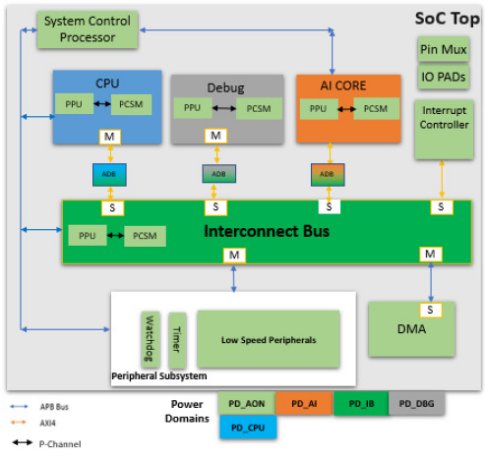
Figure 8: Low power SoC Block Diagram
The figure above is used for illustration. It shows different power domains that are supported in the SoC design implementation. The design operates on a single voltage domain. Each subsystem is interfaced with Interconnect Bus via Access Domain Bridge for handling Power Domain crossing functionality. The below table lists down the different power domains and the modules associated to these power domains:
| Power Domain | Purpose |
|---|---|
| PD_AON | Always ON Power domain. |
| PD_AI | AI Core Power domain. |
| PD_IB | Power domain for Interconnect Bus. |
| PD_NIC | Separate power domain assigned to NIC400 Fabric |
| PD_BMEM | Boot Memory is maintained in separate Power domain |
| PD_CPU | Separate power domain for CPU Subsystem |
| PD_DBG | All the Debug logic will be in this power domain |
Table 4: SoC Power Domain
Low power design for the above block diagram is maintained in two hierarchies:
- Subsystem Hierarchy: Each Subsystem of SoC instantiates PPU and PCSM. Each PPU in a subsystem controls the power domain state of the modules within that subsystem. PPU is instantiated to meet the low power design requirement for that subsystem. PPU Q-channel interface will be connected to ADB slave Q-channel for handling power state transition request and acknowledgement.
- Top Hierarchy: Power Control Module (PCM) is instantiated in System Control Processor at the Top level and sends control messages to PPU to change power state via APB interface. PCM consists of a low power FSM firmware to handle the low power state transitions for the subsystems in the SoC via Q-channel interface.
6.3 Low Power Design in Subsystem-Level Hierarchy
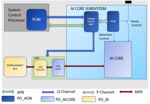
Figure 9: AI Core Block Diagram
The above AI Core subsystem level block diagram depicts how different low power components can be integrated to implement low power functionality for a specific subsystem environment. Here PPU is interfaced using APB interface with PCM for programming the PPU registers. Based on the programming, the PPU supports required power modes for a particular subsystem. PPU is also interfaced with ADB and PCM using Q-Channel interface to ensure device quiescence. For instance, when AI Core is in ON power mode, the interconnect bus must also be in ON mode to avoid any fly-off transactions. This will be controlled by ADB and PCM.
PPU and PCSM are a part of ALWAYS_ON power Domain. AI core is included under Power shut off domain i.e. PD_AI power domain. Access Domain Bridge(ADB) is placed between AI Core and Interconnect Bus to handle power domain crossing. ADB Slave and ADB master are placed in PD_AI and PD_IB power domains respectively. The ADB slave receives transfers from an AI master through AXI4 interface and the master domain transmits transfers to SCP through AXI4 interface.
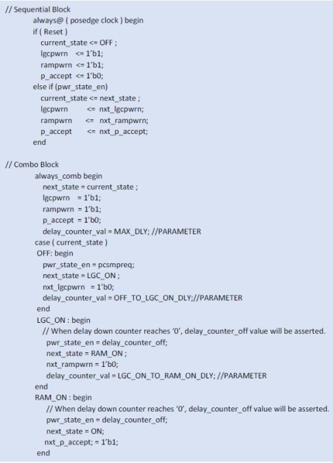
For the above AI core subsystem, assume that the PPU supports ON and OFF power modes. However, for transitions from ON to OFF or OFF to ON, the PCSM should undergo necessary transition sequence as mentioned in Table 4: Power Mode Transitions.
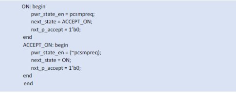
Below is the example pseudocode for above stated power mode transition that the PCSM performs:
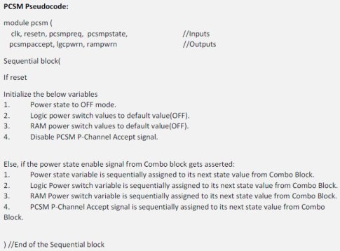
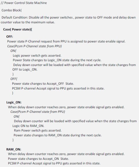
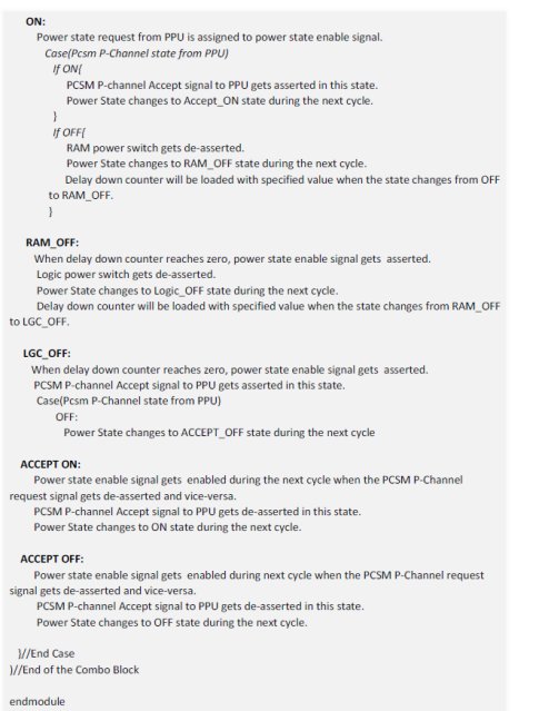
Following gives an example how the sequential and combo block logic can be implemented for a power transition from OFF to ON in Power Control State Machine Design:
The below block diagram shows how other low power interconnect components and controller components can be used to provide low power functionality:
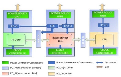
Figure 10: Low Power Interconnect and Controller Components in SoC
This Design Implementation uses PPUs for decentralized power-state transition management for each component in separate power domains. PPUs are interfaced with higher-level SCP and with PCSM for power state requests, transitions, logic and RAM retentions. Low Power Distributor-Q Channel(LPD-Q) components are used to distribute the power state transition requests to multiple design components of a particular subsystem. Low Power Combiners(LPC-Q) are interfaced with ADB to bring them to quiescence before either of the power domains are powered down. LPC components also allows two or more Q-Channel controllers to control one or more devices that all have the same control requirements. ADBs are provided for power domain crossing. Clock Controller components (CLK-CTRL) are interfaced with each device component to provide high-level clock gating mechanism.
7- Conclusion
In conclusion, we have seen the different low power strategies that are applied to a typical SoC design. We have also seen in detail the different ARM provided low power components that are employed for enabling low power functionality. In addition to this, we have also given an example on these components come together in a typical SoC.
8- References
1] Arm® CoreLink™ PCK-600 Power Control Kit Technical Manual
[2] Arm® Power Policy Unit Specification
[3] Arm® SSE-123 Example Subsystem Technical Manual
[4] Arm® CoreLink™ SSE-200 Subsystem for Embedded Technical Manual
[5] AMBA® Low Power Interface Specification ARM® Q-Channel and P-Channel Interfaces Specification
[6] P. Zhao and Z. Wang, "Low power design of vlsi circuits and systems," 2009 IEEE 8th International Conference on ASIC, 2009, pp. 17-20.
[7] B. Padmavathi, B. T. Geetha and K. Bhuvaneshwari, "Low power design techniques and implementation strategies adopted in VLSI circuits," 2017 IEEE International Conference on Power, Control, Signals and Instrumentation Engineering (ICPCSI), 2017, pp. 1764-1767
