By Aashana Pancholi, Kishan Prajapati (eInfochips)
Abstract
This paper provides a complete solution to the GPIO Verification for any SoC. GPIO interface is available in every ASIC. To avoid duplicate efforts and (save) time to verify the GPIO interface, we have produced this Generic GPIO verification suite. It is a UVM-based verification environment, with all the necessary subcomponents that are required to verify any GPIO design. It also consists of a tailored sequence library that can be used as per the design requirement. Also, we have implemented checkers and assertions in the suite to majorly check for GPIO out reset value, for posedge interrupt or negedge interrupt, and perform the required connectivity checks.
Introduction
General-purpose Input/Output (GPIO) is an interface available on most ASICs to provide ease of access to the device's internal properties. There can be several GPIO pins that depend on the application of the chip.
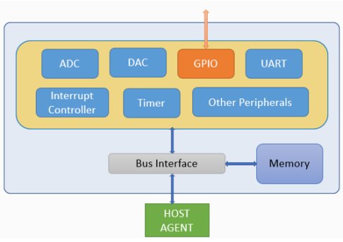
Figure 1: GPIO in a System
The pins can be programmed as input, where data from some external source is being fed into the system to be used by the host, CPU, or any other master at the desired time. The pins can also be programmed as an output, where formatted data can be transmitted efficiently to outside devices by host, CPU, or any other master. In many applications, the GPIOs can be configured as interrupt lines for a CPU to signal immediate processing of input lines.
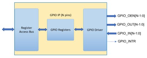
Figure 2: General GPIO IP
Every system contains such GPIO IP, and we need to put effort and time to create verification components to verify the GPIOs. To avoid duplicate effort spent on different projects, a generic GPIO verification component helps users to easily integrate and start with quick verification at the unit level, subsystem level, and SoC level using this Generic GPIO verification suite. It consists of all the necessary subcomponents required to verify any GPIO design, and the GPIO test suite, which is a tailored sequence library and can be used as per the design requirement.
GPIO Verification Suite Architecture
This is a Tailored UVM methodology-based verification component. A minimum number of UVM components are required that results in efficient compile-time and simulation time. This verification suite removes the need for multiple sequencers to take care of parallel driving and parallel sampling of GPIO pins.
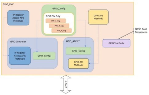
Figure 3: GPIO Verification Suite Architecture
As shown in the figure above, the verification environment contains mainly three components ─ GPIO agent, GPIO controller, and GPIO test suite.
Generally, in any of the GPIO testcase, there are two main activities. First, to drive and sample the GPIO pins from the interface, and second, configurations of GPIO IP register. The second procedure is project-specific and can vary DUT by DUT based on the bus interface.
In the GPIO verification suite, we need separate components that can perform these activities. Hence, we have both an agent and a controller. Here, the agent performs the interface level activities of sampling and driving the GPIO pins, which remain the same irrespective of the project whereas the controller handles the IP register configuration-related activities based on the bus interface specification. GPIO test suite contains some general test sequences that can be used for the verification of any GPIO. At any given point in time, based on any requirement, the user can create new testcases using the APIs provided.
Features and Functionality
The Generic GPIO verification suite allows us to verify the following features in a GPIO design:
- The configurable number of GPIO pins.
- The configurable width of address and data registers.
- Accessibility of GPIO pins through APIs.
- A test suite that covers sequences for all the general features of the GPIO.
- Supports the clock drive on GPIO pin configured as an input.
- Generic GPIO assertions and checkers.
- Supports the creation of miscellaneous testcases based on the APIs.
GPIO configuration is a wrapper class and contains an array of pin configurations. There are several configurations available by which different pins can be configured for input or output and their logic level is set as active high or active low. Also, the configuration of high time and low time is available if one needs to drive the GPIO pin as the clock.
GPIO interface contains the parametric arrays for GPIO in and GPIO out. It has the interrupt pin to be connected to the GPIO IP interrupt. This interface is connected to the DUT and hence the GPIO agent uses the interface to drive and sample the data from DUT.
The test suite consists of various GPIO sequences in the form of tasks. These tasks can be called using hierarchical reference. Some of the overviews of the testcases available in the test suite are mentioned below:
- Input configuration test in which all the GPIO pins are configured and checked for input functionality.
- Output configuration test in which all the GPIO pins are configured and checked for output functionality.
- A random configuration test in which random GPIO pins are configured and checked for input or output functionality. This process is repeated multiple times based on the test arguments.
- Interrupt test where all the pins are configured as an input. Pins are driven randomly several times to check the interrupt behavior as required. This test can be configured for active high or active low interrupts per pin.
- Walking input configuration test, where pins, one after the other, are configured and checked in the input mode. At a time, only one pin is in the input mode.
- Walking output configuration test, where pins, one after the other, are configured and checked in output mode. At a time, only one pin is in the output mode.
These sequences have several steps involving interface level and register level operations. Thus, the APIs are called from GPIO environment class. So, the GPIO environment behaves as a bridge to decide between the interface level operation or register level operation. Based on the operation, the environment shall call the appropriate API from the GPIO agent for the interface level operation or call the appropriate API from the GPIO controller in case of register level operation.
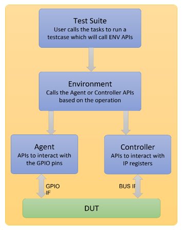
Figure 4: Functional Flow Diagram
The GPIO agent has access to the GPIO interface via virtual interface and can perform the GPIO interface activities as per the request from the test suite sequence of the miscellaneous test. The GPIO agent contains the APIs to drive the single pins or multiple pins and similarly sample single pin or multiple pins along with comparing logic.
The GPIO controller is a virtual class, that needs to be extended to override the prototype register level tasks based on the requirement. In the extended class, any other component or object can be imported to perform the register write and read operations. The controller contains the APIs to configure the GPIO configuration in DUT, write onto the GPIO output register, read, and compare the GPIO input register. Here, only required tasks need to be overridden.
All the tasks in the agent and the controller are generic as they use the parameter to indicate the number of GPIOs based on the project specifications.
Steps to Integrate
Here, steps of integration of the GPIO environment are given under the assumption that the verification environment for the DUT is already developed. The environment for the DUT is mentioned as the top environment.
- Take the instance of the GPIO environment in the top environment and create it in the build phase.
- Create and configure the GPIO configuration and set it to the GPIO environment using the hierarchical reference to get them during the build phase. The individual pin configurations for each GPIO are set here based on the DUT specifications.
- Take the instance of the GPIO interface in the verification top module. Make sure to set the number of GPIO pins parameter to replicate the exact numbers of GPIO pins available for the DUT. Connect the GPIO interface pins with the DUT. Also, set the virtual GPIO interface to the GPIO agent using hierarchical reference so that the pin-level activities to be performed by the agent can get those references.
- Extend the GPIO controller component to override all the required prototype APIs as per the DUT and top verification environment requirement so that the controller can perform the register level activities.
- Once the registers are configured, we shall override the verification suite’s GPIO controller with the top environment controller using the UVM Factory Override method.
- The GPIO verification suite is ready to run the test cases. Testcases can be run by hierarchical reference from the GPIO environment.
An example here shows the GPIO verification suite integrated with an APB Interface for ARM GPIO IP. Here, the extended GPIO controller needs to get access to the APB environment to perform the register activities, and thus, all the required testcases from the test suite can be run ARM GPIO IP.
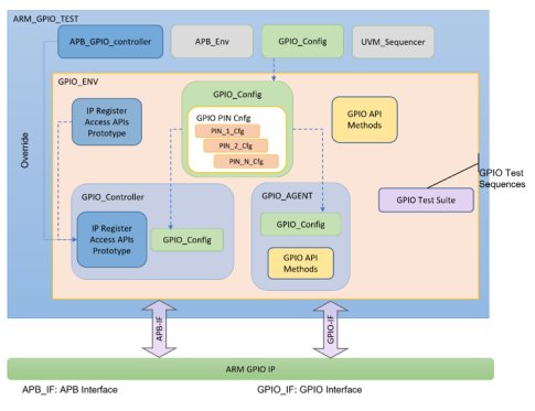
Figure 5: GPIO Verification Suite implementation example
Conclusion:
GPIO block is normally used in almost all SoCs. Generally, there are multiple GPIO pins on a single chip for the use of multiple interactions, so we see the simultaneous application. This verification component architecture for verifying the GPIO design is a complete solution for quick and detailed verification of the GPIOs. Since it is generic, a lot of effort and time are reduced. It helps in performing unit level and SoC.
eInfochips have in-depth expertise in validation and verification testing diverse systems for functional behaviour, compliance to specifications, performance and interoperability. We focus on thorough product validation while optimizing the overall regression and execution time. Combining our expertise in ASIC design verification, model-based design, design validation/verification testing, and advanced verification methodologies, eInfochips also offers a portfolio of custom Verification IPs for standard interfaces for various industries. To know more about our offerings please reach out to us today.
About the Authors
Aashana Pancholi
Aashana Pancholi is working as an ASIC Verification Senior Engineer (Level 2) at eInfochips. She has an experience of around 5 years in ASIC Design Verification at both SoC and IP level functional verification working with multiple clients. She is currently working on SoC functional verification.
Kishan Prajapati
Kishan Prajapati is working with eInfochips as an ASIC Verification Technical Lead (Level 2). He has industrial experience of 9 years in ASIC Design Verification and hands-on working experience in the verification domain at both IP and SoC levels as well as emulation using the Cadence tools. He has worked with multiple clients and is currently working on SoC functional verification.
References:
