By Pratap Narayan Singh, Adeel Ahmad (Vervesemi Microelectronics)
Analog to digital converters have three key input ports along with data output ports as per digital resolution requirements. These inputs ports are Analog Signal, Reference and Clock. If we compare across most of the converter architectures then clock frequency is directly related to output data rate and latency of the data conversion. The converter output data rate is same as sampling rate for Nyquist converters, provided ADC core is not incorporating any decimation or filtering to improve noise. Time interleaved converters take advantage of latency property to improve the sampling speed by adding more converters in parallel along with time shifted sampling clocks. This is very effective as there is a fundamental limit to the maximum sampling speed with single channel and it can be process technology dependent. There are multiple research publications discussing and comparing the advantage of the interleaving as compared to single channel converters in terms of power consumption.

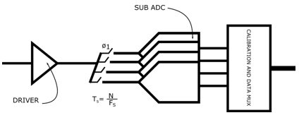
Figure 1: Interleaved ADC
As shown in Fig.1 each converter is running in parallel with sampling clocks are shifted in time to perform effective sampling at FS. This parallel operation is effectively increasing the sampling speed by a factor of N where N is number of channels. But there are some channel mismatch parameters which introduce errors when data from each channel is combined. These errors are called channel offset, gain, timing skew and bandwidth errors. These errors need to be removed before data is combined to improve the ADC performance and this is done either in foreground by interrupting the input conversion operation or in background where converter data is error free after certain time. Following sections of the article will discuss pros and cons of both methods.
Interleaving Errors:
There are mostly two type errors happen in sub-ADCs and they get converted to the gain, offset or skew errors. It’s important to understand the nature of these errors, one of the errors is static in nature and mostly contributed by process or fabrication issues like MOS or capacitor/resistance matching and they don’t change with voltage or temperature by significant amount. Most of the times process models also don’t include such variations and they are difficult to simulate as well and second type of the errors are dynamic in nature like charge feedthrough, kickback or bias drift. This kind of dynamic errors are producing the converter errors which are changing with temperature and power supply voltage and if they are not adapted with change then they will result in degrading the ADC overall performance. First kind of the errors are easy to handle because of static in nature.

Figure 2: Time domain example of errors

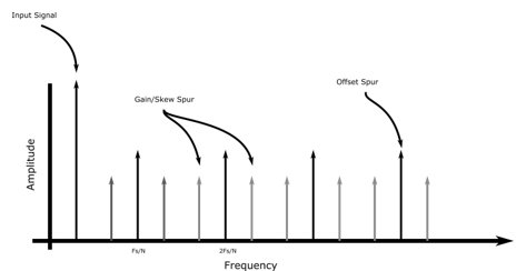
Figure 3: Errors in Frequency Domain
Foreground Calibration of the Interleaved ADC:
To perform the foreground calibration ADC conversion process is required to be interrupted and it can be achieved in some application scenarios like RF receivers where reception can be stopped during transmission phase and in this particular case calibration process is at the mercy of the transmission interval. There are certain other requirements like some predefined input signal profile or certain configuration of the converter circuitry. In first case pre-defined input signal is applied and offset, gain and timing skew is estimation is performed. For example, offset can be estimated by converting the differential input terminal shorted together and gain can be estimated by connecting the scaled references at the input and timing skew can be estimated by applying wideband or high frequency RF reference input. There are many other methods which are discussed in detail in currently available literature. But foreground calibration methods have some drawbacks like precision of the reference signals used for calibration or noise added along with additional complexity in the converter design because of need of extra circuitry. The advantage of the foreground methods is that it does not need any specific input signal signature or certain signal amplitude to complete the conversion process. But busy signals are most of the time available in communication applications because of the AGC loop. Foreground calibration is preferred for static errors and dynamic errors must be calibrated after short intervals or by detecting the change voltage and temperature otherwise it can result in unpredictable ADC behavior with time.
Background Calibration of the Interleaved ADC:
Background calibration is one of the most preferred method for the calibration of interleaving errors but it has its own limitations and depending upon application, it is decided which method is to used. There is another variation of background calibration where extra channels are used to replace the channel under calibration to stop the interruption of the normal conversion process but it comes at the cost of the design complexity as analog mux is needed most of the time at the input in this case and PPA.
Gain and offset errors look most straight forward to correct but in interleaving scenarios depending upon input signals where we can assume a very coherent scenario, the sampled signal can result as static very low frequency gain and offset errors as each channel sampling at Fs/N, the near frequency input signal can be seen as offset error by digital calibrator if there is no feedback. Similar is the case for gain errors in some multi tone scenarios where digital calibrators see it as gain errors when these input tones are close to Fs/N. So sometimes calibration schemes have to be selected based on type of the input signals profile.
There are following background methods used in calibration of the interleaved ADC
- Pure Analog Domain
It’s mostly used for calibrating the channel offset errors using DC servo loops. It has increased complexity and area increase and sometimes complete channel cannot be calibrated and it also has noise impact on overall channel.
- Blind Digital
There have been many successful efforts in calibrating channels for all errors independent of any modifications in the sub channel design of the ADC. There are some limitations like limit on input signal bandwidth, need of busy signals to access full output range, added filters changing phase response of the input signals.
- Analog Assisted Digital
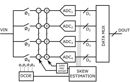
Analog assisted digital calibration is most popular and preferred method to achieve calibration in background. This is done taking help from analog domain injection of filtered signals where servo loops are implemented in digital domain and feedback is provided to analog with extracted information on errors.

Figure 4: Calibration in analog assisted digital system
What to plan as interleaved ADC calibration features:
There are some basic checks which need attention while planning a calibration system.
- How does it perform for offset and gain errors when input is beat frequency of sub channel sampling or close signal images centered around sampling frequency of sub channels and its multiples?
- How much is unusable bandwidth in the converter Nyquist range?
- How does it perform when it is out of power down and standby and calibration time after power up?
- How does gain/offset and skew calibration perform close to Nyquist of sub channels with single tone inputs?
- What is the calibration time and behavior with temperature and supply changes and supply noise?
- How does it perform with long term small integrated in-band signal power?
Vervesemi Analog to Digital Converters:
Vervesemi multi-GHz ADCs are using proprietary calibration schemes which can handle many generalized inputs signals profile and there are almost no restrictions on input signal profile as it is based on analog assisted digital calibration. These ADCs can also work with single tone signals as well as multi tone signals. Vervesemi interleaved ADCs successfully address all necessary look for features.
About Vervesemi:
Vervesemi is a fabless semiconductor company developing high performance ASICs for sensors and wireless, exploiting the expertise of state-of-art data converters and differentiated Analog IP
