By M31 Technology
Abstract
MIPI is the abbreviation of "Mobile Industry Processor Interface". This article will introduce the physical layer specifications of MIPI architecture, and explain the features and benefits of D-PHY and C-PHY respectively. Then, the MIPI perspective on the development and challenges of automotive electronics and the professional MIPI technical services that M31 can provide will be shared.
MIPI and Physical Layer IP Structure Diagram
The MIPI Association is an open membership organization founded in July 2003 by Texas Instruments (TI), STMicroelectronics (ST), ARM, and Nokia. Over the past decade, this standard has flourished and is used in a large number of applications in mobile devices such as cell phones and wearable products, including displays, lenses, storage, bridging and other signal transceivers, all of which adopt the standards set by the MIPI Association. Today, MIPI has been introduced into artificial intelligence and automotive electronics applications, and is closely integrated with all kinds of electronic products used in human life.
In the MIPI architecture, there are Application Layer, Protocol Layer and PHY Layer. In which, the physical layer is responsible for handling the signal transmission in the physical lane. In the M31 physical layer IP block diagram (Figure 1), it mainly contains two parts, PCS (Physical Coding Sub layer) and PMA (Physical Medium Attachment).The PCS uses the PHY Protocol Interface (PPI) to communicate with the MIPI controller for data transmission and various mode switching; the PMA contains the analog circuits required for external transmission, including the clock generator, transmitter, and receiver, etc. The M31 maintains a standardized design for the PPI part to improve compatibility with the controllers of major MIPI manufacturers. On the other hand, we have also reserved some special sideband control signals to meet customers' needs for diverse applications.
With the increasing amount of signal data, the MIPI Association has proposed a series of physical layers, including M-PHY, D-PHY and C-PHY, in addition to improving the operation speed. In the following sections, the features and benefits of D-PHY and C-PHY are further introduced.
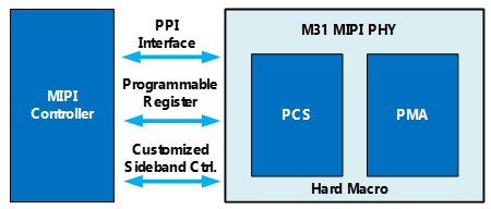
Figure 1: M31 MIPI Physical Layer block Diagram
D-PHY Features and Advantages
The D-PHY architecture consists of one clock lane and one or more data lanes, where the clock lane is unidirectional and the data lane can be unidirectional or bidirectional. The physical layer is divided into three operating modes: HS (High Speed), LP (Low Power), and ALP (Alternate Low-Power); HS mode is a low-voltage differential signal with a maximum transmission rate of 11Gbps according to the latest D-PHY v3.0; LP mode is a single-ended signal for low-speed transmission (<10Mbps) and relatively low power consumption; ALP mode is a low-speed transmission through the HS circuit module to shorten the waiting time of the system during the switching process between HS and LP. By combining various modes, the D-PHY power consumption can be optimized, and the high-speed DDR (Double Data Rate) signal is transmitted from the transmitter to the receiver through the clock lane, which makes the CDR (Clock and Data Recovery) circuit design at the receiver much easier.
In terms of bi-directional data lane function, it can be applied to Escape Mode as well as the transmission of status and display module information. There are two types of bi-directional transmission, which are Control Mode Lane Turnaround based on LP mode and Fast Lane Turnaround based on ALP mode, the former being the traditional implementation and the latter being the new one proposed after D-PHY v2.5. Fast Lane Turnaround has the ability to switch between unidirectional and bidirectional transmission without the waiting time required to enter and exit LP mode, and although it requires the addition of a high-speed transceiver circuit to the transmitter and receiver, but the improvement to overall data throughput is phenomenal. The M31 IP supports both of these bi-directional transmission modes, and optimizes the circuit layout area simultaneously.
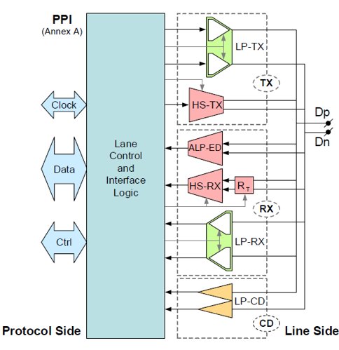
Figure 2: D-PHY Lane Module System Diagram
C-PHY Features and Advantages
Due to the increasing amount of signal data, C-PHY was developed with the structure of an A/B/C three-lane system, where the clock is embedded in the data signal without any clock lane, so as to increase the bandwidth and encode the data. First, the 16-bit signal is converted into seven symbols, each of which is transmitted through three lanes, and five Wire States Transitions are achieved using six Wire States, as shown in Figure 3 in the C-PHY datasheet. Every 3 bits of signal determines the next wire state transition, where Flip represents the positive and negative change of the signal while the wire state remains unchanged, Rotation represents the clockwise or counterclockwise change of the wire state, and Polarity represents the positive and negative polarity change of the wire state.
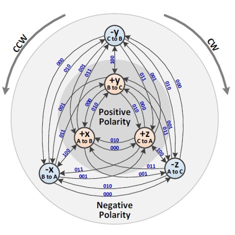
Figure 3 C-PHY Wire State Transition Diagram
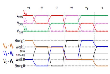
Figure 4 C-PHY HS Signal Waveform Diagram
The physical layer is also divided into three modes of operation: HS mode is a low-voltage three-phase symbolic coded signal, and the conventional differential signal is obtained by pairwise subtraction (Figure 4), with a coding gain of 2.28 (16/7). According to the latest C-PHY v2.1, the maximum transmission rate is 8Gsps; LP and ALP modes are similar to D-PHY. The bi-directional transmission also supports both Control Mode Lane Turnaround and Fast Lane Turnaround. C-PHY eliminates the clock lane, improves EMI (Electromagnetic Interference) that exists in D-PHY, further reduces the required power consumption, and achieves signal throughput by reducing pin count through coding gain (Figure 5).
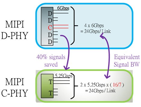
Figure 5: C-PHY/D-PHY Pin Count
MIPI in Automotive Electronics Development and Challenges
In recent years, the demand for automotive electronics applications has increased significantly. Compared with consumer electronics, the difference is that there are strict requirements for safety and reliability standards such as high temperature resistance and failure rate; therefore, the development of automotive IP must take into account the certification specifications such as AEC-Q100 and ISO26262, and pass the relevant functional certification. In addition, MIPI is also widely used in automotive applications, including display applications such as navigation, center console, dashboard, and entertainment systems; camera-side applications such as panoramic view detection, driving status monitoring, ADAS, etc.
Currently, M31 has obtained ISO26262 certification for MIPI M-PHY, MIPI D-PHY Transceiver IP and design flow, and will be able to provide high quality IP with ASIL-B specification.
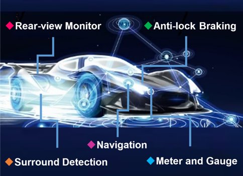
Figure 6: In-vehicle application diagram
M31 Professional MIPI Technical Support
M31 has been working in the MIPI field for 10 years and has a professional technical team that provides technology nodes from 55nm to 5nm. The team not only focuses on IP development, but also has complete technical support services. M31 has extensive experiences in cooperating with multimedia chip design companies such as display technology, smart image detection, and even automotive electronic chip design companies, and has built a complete measurement facility, from signal quality analysis, electrical characteristics measurement to system compatibility testing, to maintain close cooperation with customers. So far, M31 has a complete layout in the MIPI field for different needs, and can propose chip design optimization solutions for product applications to further enhance the competitiveness of customers' products.
