By Meetu Sharma, Afia khan (einfochips)
Abstract
I2C is a two-wire, bidirectional bus protocol that enables effective communication between one master (or multiple masters) and one or more slave devices. It is a straightforward, half-Duplex, bidirectional protocol. This paper covers the timing specification of I2C (Inter-Integrated Circuit) bus protocol. We have described all the timing specifications and how they are achieved by constraining our design. This paper focuses on the timing constraints for fast mode plus (The data transfer rate is 1 Mbit/s).
Introduction
I2C (Inter-Integrated Circuit) is a serial communication bus interface connection protocol used by devices. Philips Semiconductor created it at first in 1982. The protocol is now widely used for short-distance communication. It uses a two-wire interface with a bidirectional serial data line (SDA) and a unidirectional serial clock line (SCL). Data is transferred at rates of 100 kbits per second in Standard Mode, 400 kbits per second in Fast Mode, 1 Mbits per second in Fast Mode Plus, and up to 3.4 Mbits per second in High-Speed Mode. Several masters and slaves can be connected simultaneously in I2C, but the most common configuration is a single master and many slaves. Master is the one which is responsible for generation of clock signal, initiation and termination of transfer. The device that a Master addresses is referred to as a Slave. As all I2C addresses are either 7 bits or 10 bits so the max number of slaves can be 128 for 7 bits addressing or 1024 for 10 bits addressing.
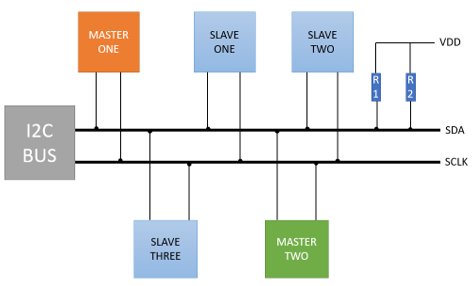
Figure 1.1 : I2C bus communication
1- I2C supported frequencies
- Standard mode: I2C in this mode goes up to the speed of 100 kilobits per second.
- Fast mode: The maximum speed is 400 kilobits per second for this mode.
Both the above modes are widely supported.
- Fast mode plus: It permits communication at the rates of 1 megabit per second. For this mode drivers might need extra strength to keep up with the quicker rise and fall times.
- High-Speed Mode: Data rate is 3.4 megabits per second in high speed mode. In order to enable this mode, the master device must first employ a master code to enable high-speed data transfer.
- Ultra-Fast: It can transfer data at a rate of up to 5 megabits per second and is the fastest mode of operation. It is write-only mode and removes some I2C features in the communication protocol.
2- Working of I2C communication protocol
I2C makes use of SDA and SCL, which are 2 bi-directional open-drain lines for data communication.
Serial Data (SDA) – Data transfer takes place via this pin.
Serial Clock (SCL) – Clock signal is carried by this pin.
It works in 2 modes –
Master: The device that drives the SCL clock line
Slave: The device that responds to the master are the slaves. Only a master is able to start a transfer on an I2C bus.
As per I2C protocols, the data line will not change when the clock signal is one, it will change only when the clock signal is zero.
Data transmission takes place in the form of packets.
Start Condition – 1 bit
Slave Address – 7 bit
Acknowledge – 1 bit
Stop condition – 1 bit
Each message has an address frame that contains the binary address of the slave. The message also contains read/write bits, ACK/NACK bits, and conditions for the start and stop of each data frame:

Figure 2.1: I2C Frame for communication
2.1- Start and Stop Condition:
By maintaining a high SCL line and varying the SDA level, START and STOP can be produced. The SDA is changed from high to low while the SCL remains high to produce the START condition. To produce STOP condition SDA changes from low to high while maintaining the SCL high.
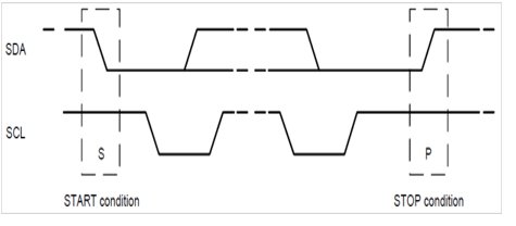
Figure 2.2: start and stop condition.
2-2- Addressing
Unlike SPI, I2C lacks slave select lines. This is achieved by addressing. The first frame in a new message after the start bit is always the address frame. Master is connected to several slaves and slave address is send by the master to each slave and this address matches with the slave address it wants to communicate. Each slave has a unique 7 to 10 bit sequence that recognizes the slave when the master wants to communicate with it. After this salve matches the address send by the master to its own unique address. When the address matches successfully, a low voltage ACK bit is send back to the master. If it doesn’t match, the slave remain ideal and do nothing, and the SDA line remains high.
2.3- Read/Write bit
The master sends the data to slave when Read/Write bit is high and receives the data from the slave when Read/Write bit is low.
2.4- Ack/Nack bit
After each data frame, follows an ACK/NACK bit. Receiver sends the ACK bit to the sender when the data frame is received successfully.
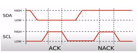
Figure 2.3: Acknowledge and Non acknowledged bit
The first data frame is prepared for transmission once the master recognises the ACK bit from the slave. The most significant bit is sent first and the data frame is always 8 bits long. An ACK/NACK bit is immediately send after each data frame to confirm that the frame was successfully received. The next data frame cannot be sent until the ACK bit has been received by either the master or the slave (depending on who is sending the data). The transmission can be stopped by the master sending a stop condition to the slave after all the data frames have been sent.
2.5- Repeated start condition
None of the master can use the bus for communication amidst each start and stop condition pair
as the bus is considered busy. A new start condition is issued by the master in order to start a new transfer without releasing the bus and this new start condition is termed as REPEATED START CONDITION.
Figure 2.4: Repeated start condition
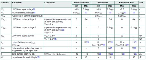
3- Characteristics of SDA and SCL I/O stages
Table 3.1 : characteristic of SDA and SCL I/O Stages
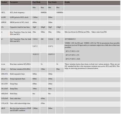
4- Timing specifications of SDA and SCL bus lines
Table 4.1 : Timing specifications of SDA and SCL bus lines
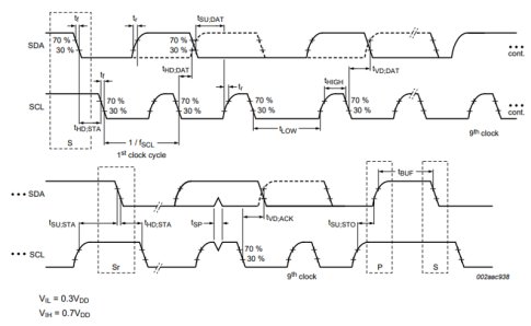
Figure 4.1 : Timing waveform of SDA and SCL bus lines
5- Constraints to achieve I2C timing specifications
The amount of time that data must be stable before being sampled is known as setup time. Typically, this period occurs between the rising SCL edge and the state change of the SDA. On the other hand, hold time is defined as the time interval after sampling has been initiated. Typically this interval is between the falling SCL edge and SDA changing state. It is important that data be held stable during these intervals as failure to do so would result in data being sampled improperly.
The I2C standard specifies the minimal time needed in these intervals for both the START and STOP conditions, as well as for data bits. Fast mode plus operating speed is taken into consideration while defining the constraints for all these timing checks.
5.1- Rise and fall transition time
Rise (tr) : The time required by the rising edge to attain 70% amplitude from 30% amplitude for each SDA and SCL is termed as tr .
Fall (tf) : The time required by the falling edge to attain 30% amplitude from an amplitude of 70% for each SDA and SCL is termed as tf
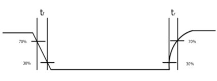
Figure 5.1: rise and fall time
5.2- Boundary conditions
Input transition
set_input_transition -rise $SCL_TR_RISE [get_ports SCL]
set_input_transition -fall $SCL_TR_FALL [get_ports SCL]
set_input_transition -rise $SDA_TR_RISE [get_ports SDA]
set_input_transition -fall $SDA_TR_FALL [get_ports SDA]
SCL_TR_RISE à min input transition from specs (20ns)
SCL_TR_FALL à (20*minVDD/5.5 + max transition variation) à (20*1.08/5.5 + 90) à 93.9
SDA_TR_RISE à min input transition from specs (20ns)
SDA_TR_FALL à 20*minVDD/5.5 à 20*1.08/5.5 à 3.9
Output load
set_load -max 130.0 [get_ports SDA]
set_load -min 30.0 [get_ports SDA]
set_load 30.0 [get_ports SCL]
5.3- Data Setup Time (tSU;DAT) (Reception constraint)
Setup time for data is defined as the minimum amount of time required for SDA to have reached a stable level before an SCL transition takes place.
This is measured between 30% amplitude of SDA during a falling edge or 70% amplitude of SDA during a rising edge and 30% amplitude of SCL during a rising edge.
tSU;DAT -> SCL-tr min; SDA-tr max
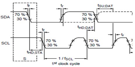
Figure 5.2: setup time of data
Required SDC Constraint
create_clock - name i2c_scl_clk -period 1000.0 -add [get_ports SCL]
set_input_delay -clock "i2c_scl_clk"-add_delay -max [expr 500 - 50] -clock_fall [get_ports SDA]
- 500 à I2C FM+ fSCL Max 1.0 MHz, Min SCL tLOW (LOW period of SCL clock)
- 50 à Setup time requirement i.e, tSU;DAT = 50ns
5.4- Data Hold time (tHD;DAT) (Reception constraint)
Hold time for data is defined as the minimum amount of time required for SCL to have reached a stable level before an SDA transition takes place.
This is measured between 30% amplitude of SCL during a falling edge and 70% amplitude of SDA during a rising edge or 30% amplitude of SDA during a rising edge.
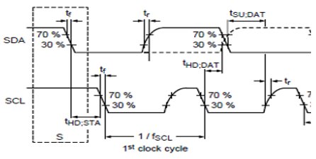
Figure 5.4: Hold time of data
Required SDC Constraints
- create_clock -name i2c_scl_clk -period 1000.0 -add [get_ports SCL]
- set_input_delay-clock"i2c_scl_ap"-add_delay -min -2 -clock_fall [get_ports SDA]
- 2ns extra margins is applied for hold check to be furtherly conservative
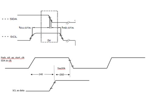
5.5- Setup time for start condition (Reception constraint)
- It is a timing specification that is only taken into account during a repeated start condition.
- The SDA line must stay high for at least this amount of time before a repeated start can be initiated.
- This is measured as the amount of time taken during transition from 70% amplitude of SCL from a LOW to HIGH and transition from 70% amplitude of SDA from a HIGH to LOW.
Figure 5.5 setup time for repeated start condition
Required SDC Constraint
- create_clock -name sdi_start_clk -period 1000.0 -add [get_ports SDA]
- set_input_delay -clock [get_clocks sdi_start_clk] -add_delay -max [expr 500 - 260] [get_ports SCL]
For start/stop condition setup and hold logic uses I2C-SDA as clock and captures I2C-SCL as data. sdi_start_clkis defined for constraining this functionality.
- 500 à I2C FM+ fSCL Max 1.0 MHz, Min SCL tLOW (LOW period of SCL clock)
- 260 à min setup time requirement for start condition i.e, tSU;STA = 260ns.Checked against $SDA rise-edge (stop logic)
5.6- Hold time for start condition (Reception constraint)
It is the minimum for which SCL should be stable at HIGH, after SDA goes low. Clock is defined at SDA and SCL is considered as data.
It is measured as the time taken from 30% amplitude of SDA from a HIGH to LOW transition to 70% of the amplitude of SCL from a HIGH to LOW transition.
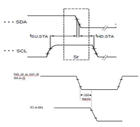
Figure 4.6: hold time for start condition
Required SDC Constraint
- create_clock -name sdi _start_clk -period 1000.0 -add [get_ports $SDA]
- set_input_delay -clock [get_clocks sdi_ start_clk] -add_delay -min 260 [get_ports $SCL] -clock_fall
- 260 à min hold time requirement for start condition i.e, tHU;STA = 260ns.Checked against $SDA fall-edge (START logic)
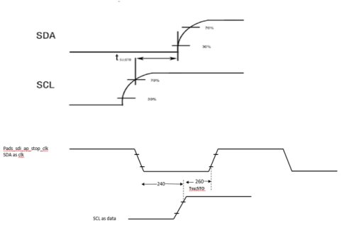
5.7- Setup time for stop condition (Reception constraint)
In a stop condition SDA transition to a HIGH state after the SCL transitions HIGH.
There is no need of hold time for a stop condition, however a minimum setup time is still required.
Setup Time for Stop Condition (tSU;STO) is measured as the time between 70% amplitude of the rising edge of SCL and 30% amplitude of a rising SDA signal during a stop condition.
Figure 4.7: setup time for stop condition
Required SDC Constraint
- create_clock -name sdi_stop_clk -period 1000.0 -add [get_ports SDA]
- set_input_delay -clock [get_clocks sdi_stop_clk] -add_delay -max [expr 500 - 260] [get_ports SCL] -clock_fall
- 500 à I2C FM+ fSCL Max 1.0 MHz, Min SCL tLOW (LOW period of SCL clock)
- 260 àmin setup time requirement for stop condition i.e, tSU;STO = 260ns. Checked against $SDA rise-edge (STOP logic)
5.8- Data Valid Time/Data Valid Acknowledge Time (Transmission constraint)
Data Valid Time (tDV;DAT)
- The validity of data is measured at every data and clock transition.
- The data valid time tDV;DAT is measured between the falling edge of SDA at 30% or the rising edge of SDA at 70% amplitude with reference to 30% of the falling edge of SCL.
Data Valid Acknowledge Time (tDV;ACK)
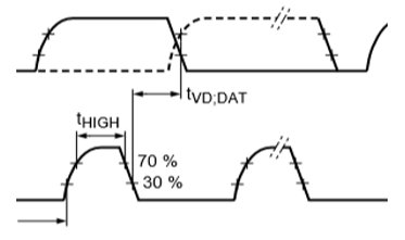
Figure 4.8 Data valid time
TX Max Delay constraints
set_output_delay -clock "i2c_clk"-add_delay -max [expr 50 + 60] [get_ports SDA]
#SCL dly - (0.5* SCL in-tr) + dig_top logic dly + SDA dly + (0.5 * SDA out-tr)
- 50 âž” 500 – 450 (tVD max 450 from UM10204 and SCL tLOW 500)
- 60 âž” Max allowed SDA out-transition from I2C Spec 120ns à assuming pessimistically 60ns contribution for output delay
Transmission Data hold time
As we know that tHD;DAT = 0 defined from {30% of SCL-fall} -> {30% SDA-rise, 70% SDA-fall so the minimum SCL->SDA delay (50%->50%) which must be guaranteed by transmitter (TX) device.
This min value is computed as: (0.5 * SCL tr) + (0.5 * SDA tr) and as a consequence depends on SCL input transition and SDA out load.
- set_output_delay -clock "i2c_scl_clk" -add_delay -min [expr (60 + 12) * -1] [get_ports SDA] -clock_fall
[expr (60 + 12) * -1]
- 60 à (0.5 * SCL tr) contribution critical case à (0.5 * 120)
- 12 à SDA tr à The actual critical case is calculated on FF PVTs, min load, 4K Rp and SDA fall tr.
Note : (0.5 * SDA tr) contribution would be max in a given PVT for max out load which on the contrary is also the condition which maximizes the SDA IO-Cell delay.
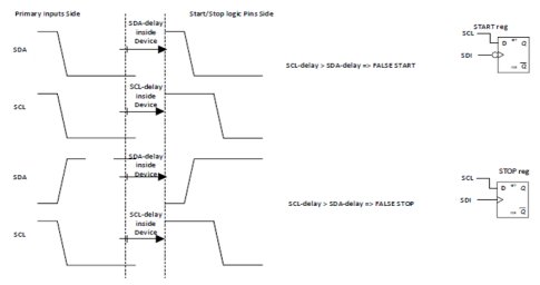
5.9 False Start/Stop due to SDA/SCL switching closely for tHD;DAT=0ns (Reception constraint)
If delay of SCL > delay of SDA, False START/STOP condition can occur.
To check, that it does not happen, we do a setup check that SCL should remain Low before SDA going Low or High
Figure 5.9: False Start/Stop due to SDA/SCL switching closely for tHD;DAT=0ns
- set_input_delay -clock [get_clocks sdi_clk] -add_delay -max [expr 500 + 2] [get_ports SCL] -clock_fall
- set_input_delay -clock [get_clocks sdi_clk] -add_delay -max [expr 500 + 2] [get_ports SCL]
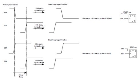
5.10- False Start/Stop due to SDA/SCL switching closely for tSU;DAT=50ns (Reception constraint)
If delay of SDA > delay of SCL, False START/STOP condition can occur.
To check, that it does not happen, we do a hold check that SCL should remain Low after SDA going Low or High
Figure 5.10: False Start/Stop due to SDA/SCL switching closely for tHD;DAT=50ns
- set_input_delay -clock [get_clocks sdi_clk] -add_delay -min 50 [get_ports SCL] -clock_fall
- set_input_delay -clock [get_clocks sdi_clk] -add_delay -min 50 [get_ports SCL]
Start condition logic operates at SDA fall edge and stop condition logic operates at SDA rise edge.
- 500 à half cycle of SCL period
- 50 à Setup time requirement i.e, tSU;DAT = 50ns
6- Conclusion
This paper presents the working of I2C protocol as well as constraint implementation. I2C is multi slave and multi-master bus and very important for communication between fast and slow devices. In this paper we analyzed the timing specifications for transmission and reception of signals using I2C protocol in fast plus mode. And defined the timing constraints that we need to provide to the implementation in order to achieve these specifications. We explained the constraints for setup(data), hold(data), setup and hold for start/stop condition, data valid time, data transmission time and also for false start/stop condition.
7- Authors

Meetu Sharma (Technical Manager)
She is a diligent Technical manager in einfochips and having experience of more than 18 years in VLSI. She has experience of working on various technology nodes such as 180nm, 110nm, 28nm, 7nm, and 3nm in physical designing SoCs and has successfully taped out ASIC chips from RTL netlist to GDS including Sign off process.

Afia khan (Engineer)
She is a PD Engineer in eInfochips working in the ASIC domain. She joined as fresher and having 1.5 year of experience in block level implementation. Her project exposure includes PnR, Static Timing Analysis and signoff checks. She owns Bachelor of Technology degree in Electronics from Rajkiya Engineering College Sonbhadra.
8- References
I2C Timing: Definition and Specification Guide (Part 2) | Analog Devices. (n.d.). I2C Timing: Definition and Specification Guide (Part 2) | Analog Devices. https://www.analog.com/en/technical-articles/i2c-timing-definition-and-specification-guide-part-2.html
Semiconductors, N. (n.d.). UM10204 I 2 C-bus specification and user manual Rev. 6-4 April 2014 User manual Document information Info Content. http://www.nxp.com
Pu, R. (n.d.). Slave or Master. www.ti.com
I2C Communication Protocol - GeeksforGeeks. (2021, February 1). GeeksforGeeks. https://www.geeksforgeeks.org/i2c-communication-protocol/


