By Agnisys
Every aspect of designing, verifying, programming, validating, and documenting system-on-chip (SoC) devices is really hard. Semiconductor companies simply cannot hire enough engineers to create each new chip from scratch. They make extensive use of design reuse, verification IP reuse, and electronic design automation (EDA) tools to shrink schedules, save time, and improve quality.
One particularly challenging stage of SoC development is verifying that the complete design has been assembled correctly. This requires checking to be sure that both the software and hardware do what they are intended to do. Automating much of this process is possible using a combination of the Portable Stimulus Standard (PSS) and Universal Verification Methodology (UVM) register models.
Registers Are Ubiquitous
Programmable registers are universal in SoC designs. They provide the hardware-software interface (HSI) through which low-level software such as drivers and embedded code configures and controls the hardware. These registers are defined as part of the chip architecture in the design specification, which is used by every team on the SoC development project.
Since natural-language specifications are inherently imprecise and ambiguous, the industry has created several formats to define registers more clearly. These include SystemRDL, IP-XACT, and, most recently, PSS. The latest version of the standard includes language constructs to specify the programmable registers in the design.
PSS was developed—and continues to be evolved—by Accellera Systems Initiative to automate more of the design verification and validation flows. The standard defines abstract, portable specifications of verification intent. PSS models enable compliant tools to generate tests that work both “vertically” from block to system and “horizontally” from simulation to silicon.
Generating Register Designs from PSS
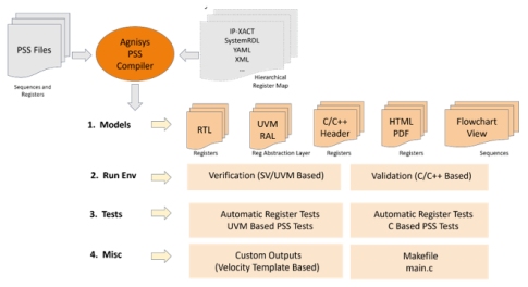
The Agnisys IDesignSpec™ family of specification automation solutions reads all standard formats and provides a specialized editor for visual register specification. The Agnisys PSS Compiler supports register and sequence specification via portable stimulus. The IDesignSpec family can also generate PSS code when other register definition methods are used, and enables mixing formats.
Whatever method is used to specify the registers, including PSS, IDesignSpec GDI and IDS-Batch™ CLI automatically generate the register transfer level (RTL) design for the registers. This frees the designer from having to hand-code this significant portion of the design, saving project resources and reducing the time to market (TTM).
The generated RTL design includes interfaces to standard buses such as APB, AHB, AHB-Lite, AXI4, AXI4-Lite, TileLink, Avalon, and Wishbone. The code also includes any necessary clock-domain-crossing (CDC) logic for asynchronous clocks as well as parity, error-correcting code (ECC), cyclic redundancy check (CRC), and triple module redundancy (TMR) safety mechanisms.
Generating Register Programming Sequences from PSS
Initializing the programmable registers, using them to configure the hardware, controlling the operation of the SoC, and gathering status all require sequences running in the low-level software. Among its many capabilities, PSS provides constructs to define sequences, including those used to configure and program registers.
Agnisys IDS-Validate™ automatically generates C/C++ code that implements the specified PSS sequences. The ability to generate both the RTL design and the programs from PSS descriptions is highly valuable. This prevents differing interpretations by the hardware and software teams, avoiding lengthy debug cycles during pre-silicon validation.
Programmers can use the generated C/C++ in several ways. The sequences can be used in the embedded code running in the SoC’s processors during both pre-silicon validation in simulation and post-silicon validation in the bringup lab. In many cases, this code is incorporated into the production versions of the embedded software or system device drivers.

Registers Must Be Verified
Pre-silicon register validation in simulation includes not just the embedded software and the RTL design, but also a testbench and tests compliant with the UVM. This validation environment directly leverages the hardware verification environment, which may not include processors executing embedded programs.
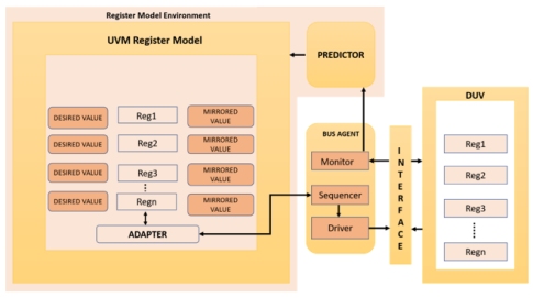
The UVM standard defines the Register Abstraction Layer (RAL) for verification purposes. The UVM RAL provides a standard library of base classes and methods, forming a high-level abstraction for reading and writing the registers in the design. The RAL also includes a test sequence library to verify the design registers.
These tests apply stimulus to the design inputs, and a monitor reads the register contents at the end of tests to check for expected results. The UVM RAL library does not include any built-in coverage model, but it provides an application programming interface (API) for the user to instantiate and sample their own coverage models.
Generating UVM Register Verification Environments
The same PSS sequences that are used to generate C/C++ code can also be used to generate the UVM sequences used in the verification and pre-silicon validation tests. Agnisys IDS-Verify™ reads PSS and automatically generates the UVM sequences required to configure and program the registers in the design under verification (DUV).
The generated tests go far beyond those included in the baseline RAL. These include high-coverage tests for hundreds of special register types, including indirect, indexed, read-only/write-only, alias, lock, shadow, FIFO, buffer, interrupt, counter, paged, virtual, external, and read/write pairs. IDS-Verify supports memories as well, instantiating models in the testbench and generating appropriate tests.
IDS-Verify also generates the complete UVM RAL verification environment, saving even more time and resources on the SoC project. This includes a driver to apply the sequences, a monitor and predictor to check test results, and auto-mirroring of the UVM register model whenever an RTL register is changed. IDS-Verify supports multiple types of coverage models, including cross-coverage.

Conclusion
The Agnisys IDesignSpec family supports all relevant standards for register design, verification, validation, and documentation. These include the well-established UVM RAL and the emerging PSS. As part of the industry’s most advanced specification automation solution, the Agnisys PSS/UVM flow is robust and proven to save time and resources not just once, but every time that a register specification evolves over the course of the SoC project.
