By Hans Bouwmeester, PrimisAI, COO
Design Productivity Gap
Twenty-five years ago, SEMATECH first alerted the world to a concern known as the design productivity gap: the observation that the ability to manufacture complex chips had started outpacing the capability of designers to create them by more than a factor of two. This concern was subsequently reiterated in the ITRS report of 1999 and discussed and reported on in many articles during the past two decades (Figure 1).
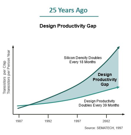
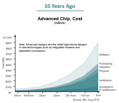
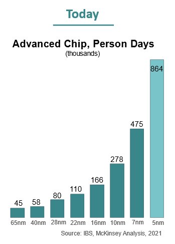
Figure 1: Design Productivity Gap
In recent years, generative AI in general and natural language processing more specifically have taken the world by storm, opening-up a wealth of possible applications, including chip design.
But will it be enough to finally start closing the productivity gap, where continuous improvements in EDA and the application of IP-reuse have done nothing more than decelerate its growth somewhat? This article presents a comprehensive overview, showing that generative AI will indeed finally close the design productivity gap and even enable us to fully automate hardware design.
Generative AI Applications in Chip Design
A first reason why generative AI helps close the productivity gap is thanks to the breadth of applications where it can be applied. This is illustrated here by distinguishing between three main categories of value-add, each with a multitude of possible applications (Figure 2).
A first category of applications relates to applying a Large Language Model (LLM) for the purpose of creation and innovation. We can deploy the creative aspects of the LLM to automatically generate, for example, architectural specifications, Verilog or VHDL code, a design with integrated IP, a verification test plan with testbench and test-cases or a configuration file for synthesis.
A second category of applications leverages the LLMs ability to help extract knowledge from information. When presented with, for example, a specification, HDL code or any kind of associated documentation, the LLM can be queried for insights giving designers the knowledge needed to determine next steps. This ability can be further enhanced thanks to a technique called RAG (Retrieval Augmented Generation) whereby the LLM is paired with a knowledge base with information it can leverage to generate its response.
A third category of applications relates to applying the LLM in boring, mundane and repetitive tasks which have proven to be very hard to automate before. Examples in this category are generating product documentation, adding comments to code, periodically reporting status and the analysis of large tool-generated log-files.

Figure 2: Example Application Areas in Chip Design
Design Intent Abstraction
Another arrow in the quiver of generative AI is that it enables us to move up to the next abstraction level as we design our chips. Where we progressed from mostly using transistor models in the 70s to logic gates in the 80s, synthesizable RTL in the 90s, design-IP in the 2000s and system design languages and TLM (Transaction Level Modeling) techniques in the 2010s, we have now started using natural language as the main language to specify our design and verification intent (Figure 3).
Note that this will not replace underlying languages like Verilog and SystemVerilog. Rather, it will become a shell around them as we can now translate a design intent expressed in natural language directly to HDL-code thus saving significant coding time and effort.
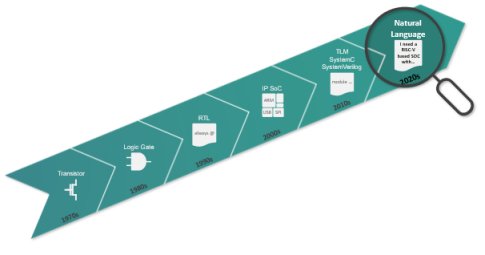
Figure 3: Design Intent Abstraction over Time
AI Agents
Although the ability to express the design intent in natural language has provided a big step forward, we are still at the humble beginnings of what the new generative AI technology has to offer. This is illustrated in Figure 4 which shows layers of technology being added to the basic conversational abilities as offered by an off-the-shelf LLM thereby transforming it into a chip design AI agent.
Using natural language as its main input and output, the agent assists with all aspects of the design creation process by combining its trained knowledge with an external knowledge base containing prior designs, IP, and associated documentation. In addition, it can call underlying EDA tools and analyze the results. It can continuously monitor the design repository for changes, enabling it to autonomously take actions, and ultimately will be able to adapt its behavior based on learnings from the past.
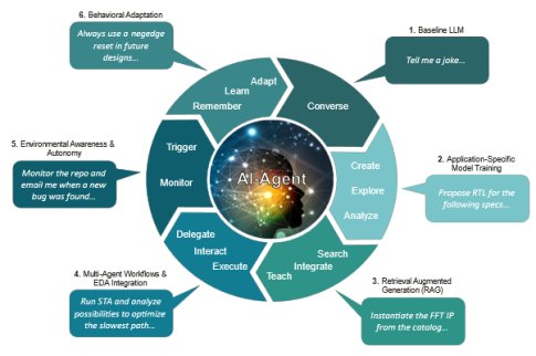
Figure 4: Evolving AI Agent Technology
Shown clockwise: (1) general conversational abilities of the AI agent are enabled by a baseline LLM; (2) the LLM is trained and fine-tuned to excel at specific applications like chip design; (3) the LLM is augmented with a (RAG: Retrieval Augmented Generation) knowledge-base containing for example prior designs, design-IP and relevant documentation; (4) the AI agent is equipped with the ability to call and interact with underlying EDA tools, as well as to call other agents in a multi-agent workflow; (5) the AI agent is deployed in an always-on, multi-tasking, operating-system like system enabling it to monitor it’s environment and to autonomously deploy initiatives; (6) the AI agent is equipped with memory enabling it to remember, learn and ultimately adapt its future behavior based on user instructions and learning from the past.
Human Involvement in Iterative Tasks
To explain why current “traditional” EDA tools have not been able to start closing the design productivity gap and how generative AI can help, we need to look at the nature of the steps needed to complete a given task. As most tasks are iterative by nature, we model the task using the well-documented Plan-Do-Check-Act (PDCA) cycle (Figure 5).
Looking at traditional EDA tools these generally do a good job at the Do-step but most often fall short at the Plan-step. An example is the design verification task where EDA tools help run simulations (Do) to detect bugs (Check). However, writing the test-plan and test-benches (Plan) and fixing any bugs found (Act) is left to the design verification engineer. This signals a need for a “human-in-the-loop” preventing us from being able to fully automate the task.
AI agents on the other hand, can help with the Plan-step. Thanks to their transformative nature, they are well suited to translate the task requirements into an executable process. For example, for the above design verification task the AI agent can transform the requirements into a test-plan with associated testbench and test-cases. It can also interpret any bug reports and automatically correct the issue (Check and Act). It can even look at code coverage reports and automatically add more test cases to automatically improve the quality of the verification regression test suite.
It is evident that traditional EDA and generative AI agents complement each other very well, in many cases enabling us to eliminate the need for human involvement when iterating over a task’s PDCA-cycle to get the best results.
Figure 5: Eliminating the Human-in-the-Loop Need in Intra-Task Iterations
PDCA: PLAN: Establish objectives and a process needed to meet them; DO: Execute plan;
CHECK: Compare results against objectives; ACT: If needed, adjust the plan and reiterate.
Inter-Task Dependencies
Although individual AI agents enable us to eliminate the human-in-the-loop for many individual tasks, the overall task of designing a chip is much more complex. To fully automate chip design, we need to deal with many inter dependent tasks where we often need to redo a task based on the outcome of a task later in the flow. For example, as the layout is already in progress, a back-annotated static timing analysis run may report that timing cannot be met requiring an adjustment of the synthesis configuration, or even the RTL code to address the issue (Figure 6).
Such inter-task reiterations can generally be addressed using generative AI as well. By having an AI agent interpret the outcome (log file) from a Do-step in the PDCA cycle (Figure 5), it can decide on what to do in the Act-step. This can involve iterating over the same task, redoing an earlier task in the flow, or proceeding with the next task in the flow.
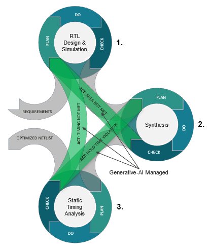
Figure 6: Automating Inter-Task Re-Iterations
Multi-Agent Workflows
To manage complex tasks, our industry is used to taking a divide-and-conquer like approach by splitting up the task into subtasks. For chip design, subtasks include architectural specification, RTL-coding, design-verification, synthesis, physical layout & verification, power & signal integrity analysis, packaging, manufacturing & test and silicon validation. Splitting up the bigger task also enables a separation of concerns as each subtask has become its own discipline, with domain experts being assigned to each phase in the overall flow.
Looking at the evolution of an AI agent as described earlier (Figure 4) we can apply the same approach by creating specialized AI agents that are experts at executing given tasks. These expert AI agents can now be deployed in a multi-agent workflow where the agents are organized to together execute a higher-level task. As the higher-level task itself can be a sub-task of an even higher-level task, we can compose a hierarchy of workflows, each executed by one or more AI agents each with a different area of expertise.
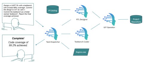
The example in Figure 7 illustrates this concept. Here, Task Dispatcher is instructed to create Verilog RTL alongside a testbench with a code overage target. Task Dispatcher interprets the request and concludes through LLM autocompletion that it first needs to prompt RTL Designer to create and check-in a first version of the RTL-code. When RTL Designer reports back it has finished this task, Task Dispatcher subsequently passes the specification and design interface description to Testbench Coder to create the verification testbench. Once this is done, Task Dispatcher runs executable “regress.exe” and analyses the results. If a bug is found in the code, it prompts RTL Designer to fix it. If the code coverage is below the target, it prompts Testbench Coder to add more tests. If the code is bug-free and the code coverage meets the target Task Dispatcher reports back that the task is complete.
Figure 7: Example Multi-Agent Workflow
Conclusion - Fully Automated Chip Design
The advent of generative AI is revolutionizing chip design. Not only does it enable us to specify our design and verification intent using natural language, but it can also be applied in many different tasks including some that were very difficult to automate before like documentation, commenting code and helpdesk support.
Moreover, thanks to the fact that generative AI and traditional EDA complement each other very well, we can eliminate the human-in-the-loop need in many iterative tasks. By organizing specialized AI agents into multi-agent workflows we can automatically manage the overall complex system of task inter-dependencies, thereby enabling us to fully automate the entire chip design process.
About PrimisAI
PrimisAI is the premier destination for cutting-edge hardware design automation, offering engineers the ultimate generative AI companion with advanced Language-to-Code and Language-to-Verification capabilities. Our interactive AI assistant called RapidGPT swiftly addresses complex hardware challenges across the entire design stack, from concept to Bitstream/GDSII. With on-premise deployment and an easily extendable knowledge base tailored to client-specific IPs, PrimisAI ensures an unparalleled hardware design experience.


