By Abhishek BV, eInfochips
Abstract:
In analog layout design, precise layout matching techniques are crucial to ensure the accuracy and performance of the circuit so that transistors exhibit similar electrical properties (i.e. transconductance, current gain, and drain capacitance). The primary purpose of these techniques is to minimize mismatches between components, which can significantly affect circuit functionality. Key techniques include a common centroid layout that helps balance process variations by placing components symmetrically around a central point and interdigitated layout interleaving devices to average out local variations. These strategies, along with careful routing and shielding, mitigate the effects of process, voltage, and temperature variations. By employing these matching techniques, designers can achieve better performance, reduce offset errors, and enhance the reliability of analog circuits in various applications.
Introduction:
LAYOUT MATCHING:
Many analog circuits depend heavily on transistor matching. For instance, differential pairs require precise gate-to-source voltage matching, while current mirrors rely on accurate current matching. Resistors and capacitors typically have a tolerance of around 20% to 30%. However, by properly matching similar components, the ratio between them can be controlled to a much tighter tolerance.
CAUSES FOR MISMATCH:
Mismatch in integrated circuits generally falls into two categories:
a) Random mismatches arise from microscopic fluctuations in dimensions, doping concentrations, oxide thickness, and other parameters that affect component values. These variations are inherently unpredictable and result from the stochastic nature of the manufacturing process.
b) Systematic mismatches occur due to process biases, mechanical stress, temperature gradients, and non-uniform current flow. These factors introduce predictable variations during the fabrication and operation of integrated circuits, influencing component performance and reliability.
Rules for MOS Transistor matching:
- Place transistors close to minimize process variations and ensure similar operating conditions.
- Orient transistors in the same direction to ensure consistent electrical characteristics.
- Keep the layout of the transistors compact to minimize process variations and maintain uniformity in performance.
- Place transistor segments in the areas of low stress gradients.
- It's advisable to place transistors well away from power devices. This separation helps minimize interference and ensures that the transistors operate under consistent and stable conditions, reducing the risk of mismatch due to varying electrical characteristics or thermal effects from high-power components.
- To achieve current matching in MOS (metal oxide semiconductor) transistors, it's beneficial to use a larger overdrive voltage. Conversely, for voltage matching, a smaller overdrive voltage is preferable. These strategies help control the operating points of the transistors more precisely, ensuring they exhibit similar electrical characteristics and performance.
Ensure that all devices experience the same process conditions and environmental factors during fabrication and operation by placing them in identical as shown in figure 1.1 below:

Figure 1.1 - illustrates transistor orientation are important.
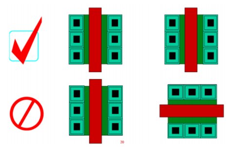
Figure 1.2 illustrates if the Orientation of the transistors is not correct then parasitic capacitance & resistance will increase which will affect the speed of the circuit.
Rules for matching Resistor and Capacitor include:
- Construct matched resistors/capacitors of the same type to ensure similar electrical characteristics.
- Make matched resistors/capacitors of the same width to minimize process variations.
- Orient matched resistors in the same direction to maintain uniform electrical characteristics.
- Place matched resistors/capacitors close to reduce parasitic effects and ensure similar operating conditions.
- Arrange the matched resistors so that their centroids coincide, using an interdigitated layout. Interdigitated arrays involve interleaving the fingers or segments of the resistors that helps to average out process variations and maintain uniformity in electrical properties.
- Place dummies on either end of the active resistors/capacitors array, shown in figure 2.1 & figure 2.2 below.
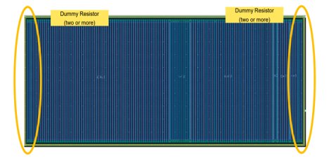
Figure 2.1 - illustrates dummy resistors are placed on either side of active resistors.
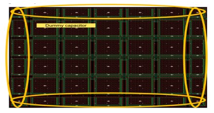
Figure 2.2 - illustrates dummy capacitors are placed on either side of active capacitors.
Dummy devices play a crucial role in enhancing the reliability and yield of integrated circuits by stabilizing the fabrication process and protecting active components from harmful etching effects. For a good, matched layout, dummy device must be used.
There are two types of device matching in analog layout namely:
- Common centroid technique
- Interdigitation technique
Common centroid:
There are four rules for common centroid layout
- Coincidence – Coincidence of centroid refers to aligning their central points as closely as possible.
- Symmetry – Symmetry around both x and y axis refers to arranging the devices in a way that their placement is balanced and mirrored both horizontally (x-axis) and vertically (y-axis).
- Dispersion – Dispersion refers to the intentional spreading or scattering of devices within an array.
- Compactness – The array should be designed to occupy as little space as possible on the integrated circuit layout.
Interdigitation: Placing alternate components.
Example 1 âž” We must match two components A and B (A and B can be anything like transistor, resistor, and capacitor). Let’s split A and B into four small components to match i.e. A1-A4 and B1-B4 which is shown in figure 3.1 below.
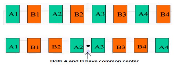
Figure 3.1 - Interdigitation and common centroid matching techniques are shown respectively.
Example 2 âž” Consider the current mirror circuit which has A=10, B=20 & C=40 multipliers shown in figure 3.2 below:
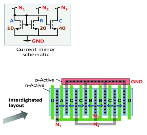
Figure 3.2 - illustrates devices B and C are splitted and distributed to 10 multipliers each and dummy (D) is placed on either side.
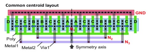
Figure 3.3 - illustrates devices A, B and C are splitted and distributed to 5 multipliers each and dummy (D) is placed on either side.
Some of interdigitation patterns for two dimensional common centroid arrays are given in figure 3.4 below:

Figure 3.4
To obtain complete matching in resistors, it should contain an even number of segments. Half of the segments connected in one direction and the rest in another direction. If the resistors have an odd number of segments, then one segment cannot be paired. The two contacts of serpentine resistor should reside close to one another to minimize the impact of thermoelectric shown in figure 4.1.
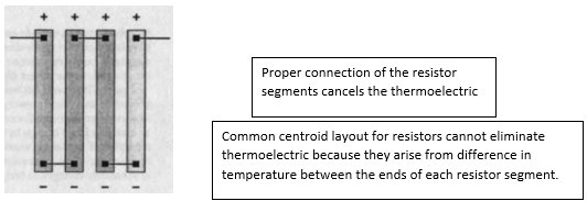
Figure 4.1 - Two contacts of a serpentine resistor placed close to each other to minimize the impact of thermoelectric effects.
Example 3:
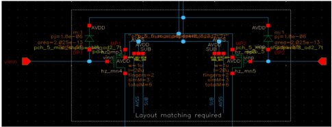
In my design, there was a differential pair having two fingers and three multipliers shown in figure 5.1. In addition, there are diodes that are added to avoid threshold voltage shifts during the manufacturing process. We should place these diodes in the same well of these transistors.
Figure 5.1
For this differential pair, matching was done in the pattern below:
Example 4:
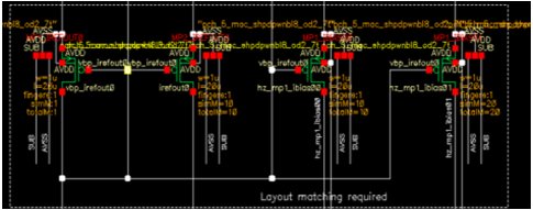
There was a current mirror having A=1, B=10, C=10, and D=20 multipliers in my design, which is shown in figure 5.2. Device A is a diode (gate and drain connection are shorted).
Figure 5.2
For this current mirror, matching was done in the following pattern:
X represents Dummy
Conclusion
Layout designer should determine which components must match and with what precision. With proper matching techniques we can avoid change in electrical properties of the components due to process variations during fabrication stage. Matched devices should never reside in the corners of the die or near major heat source. The exact degree of matching achievable from any given layout is difficult to determine. The hard data required to quantitatively evaluate matching performance is rarely available in the manufacturing environment, so the layout designer makes decisions based on limited information.
Reference: The Art of Analog layout by Alan Hastings.
About the author

ABHISHEK BV
Working as Senior Engineer in eInfochips for more than two years and having overall 6+ years of experience in Analog layout design. Graduated in Electronics and Communication engineering. He has experience of working on various technology nodes such as 7nm, 10nm, 16nm, 40nm, 65nm, 130nm and 180nm in Analog layout design and he likes to play cricket and Snooker in his free time.

